

Xem thông số kỹ thuật để biết chi tiết sản phẩm.
LFE5UM-85F-6BG756I
Product Overview
Category
The LFE5UM-85F-6BG756I belongs to the category of Field-Programmable Gate Arrays (FPGAs).
Use
This FPGA is commonly used in various electronic devices and systems for digital logic implementation, signal processing, and control applications.
Characteristics
- High-performance FPGA with advanced features
- Offers a large number of programmable logic cells and embedded memory blocks
- Provides high-speed I/O interfaces for efficient data transfer
- Supports complex digital designs and algorithms
- Configurable to meet specific application requirements
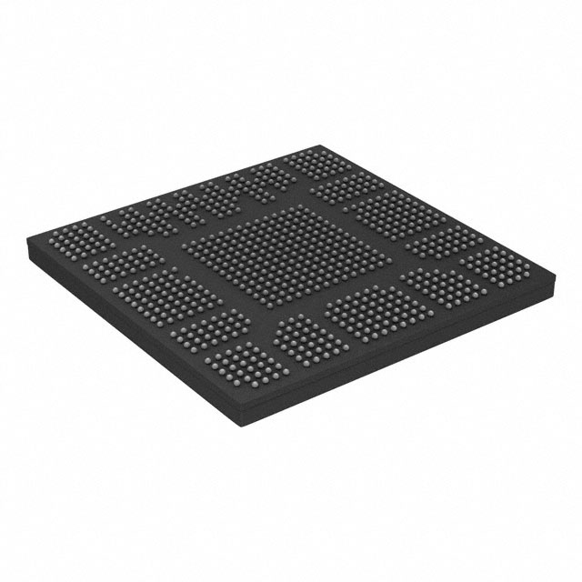
Package
The LFE5UM-85F-6BG756I comes in a compact and durable package suitable for surface-mount technology (SMT) assembly. The package ensures easy integration into electronic circuit boards.
Essence
The essence of the LFE5UM-85F-6BG756I lies in its ability to provide flexible and customizable digital logic functionality, enabling designers to implement complex algorithms and achieve high-performance solutions.
Packaging/Quantity
The LFE5UM-85F-6BG756I is typically packaged in reels or trays, depending on the manufacturer's specifications. The quantity per package may vary but is usually supplied in bulk quantities suitable for production purposes.
Specifications
- FPGA Family: Lattice ECP5
- Logic Elements: 84,000
- Embedded Memory: 4.8 Mb
- User I/Os: 600
- Speed Grade: -6
- Package Type: Ball Grid Array (BGA)
- Package Pins: 756
- Operating Voltage: 1.2V
- Operating Temperature Range: -40°C to +100°C
Detailed Pin Configuration
The LFE5UM-85F-6BG756I has 756 pins arranged in a ball grid array (BGA) package. The pin configuration includes dedicated input/output pins, power supply pins, ground pins, and configuration pins. A detailed pinout diagram can be found in the product datasheet.
Functional Features
- High-speed I/O interfaces: Supports various high-speed serial protocols such as PCIe, Ethernet, USB, and DDR3 memory interfaces.
- Flexible logic resources: Offers a large number of programmable logic cells, look-up tables, and flip-flops for implementing complex digital designs.
- Embedded memory blocks: Provides on-chip memory resources for data storage and efficient access.
- Clock management: Includes phase-locked loops (PLLs) and delay-locked loops (DLLs) for precise clock generation and distribution.
- Configuration options: Supports multiple configuration modes, including JTAG, SPI, and fast passive parallel (FPP).
Advantages and Disadvantages
Advantages
- Flexibility: Can be reprogrammed to adapt to changing design requirements.
- High-performance: Capable of handling complex algorithms and processing large amounts of data.
- Integration: Offers a wide range of I/O interfaces for seamless integration with other system components.
- Cost-effective: Eliminates the need for custom ASIC development, reducing overall project costs.
Disadvantages
- Learning curve: Requires expertise in FPGA programming and design methodologies.
- Power consumption: FPGAs can consume more power compared to application-specific integrated circuits (ASICs) for similar functionality.
- Limited analog capabilities: FPGAs are primarily digital devices and may have limited analog signal processing capabilities.
Working Principles
The LFE5UM-85F-6BG756I is based on the concept of reconfigurable hardware. It consists of an array of programmable logic cells interconnected through configurable routing resources. These logic cells can be programmed to implement desired digital functions using a hardware description language (HDL) such as VHDL or Verilog. The configuration data is stored in on-chip memory elements and can be modified to achieve different functionality.
Detailed Application Field Plans
The LFE5UM-85F-6BG756I finds applications in various fields, including:
- Communications: Used in wireless base stations, network routers, and switches for high-speed data processing and protocol handling.
- Industrial Automation: Enables control systems for robotics, motor drives, and process automation.
- Aerospace and Defense: Utilized in radar systems, avionics, and secure communication systems.
- Medical Devices: Supports medical imaging, patient monitoring, and diagnostic equipment.
- Automotive: Used in advanced driver-assistance systems (ADAS), infotainment systems, and engine control units (ECUs).
Detailed and Complete Alternative Models
- Xilinx Virtex UltraScale+ VU9P: Offers similar high-performance FPGA capabilities with a large number of logic cells and embedded resources.
- Intel Stratix 10 GX: Provides advanced FPGA features with high-speed transceivers and extensive I/O capabilities.
- Microsemi PolarFire
Liệt kê 10 câu hỏi và câu trả lời thường gặp liên quan đến ứng dụng LFE5UM-85F-6BG756I trong giải pháp kỹ thuật
Sure! Here are 10 common questions and answers related to the application of LFE5UM-85F-6BG756I in technical solutions:
Q: What is the LFE5UM-85F-6BG756I? A: The LFE5UM-85F-6BG756I is a high-performance field-programmable gate array (FPGA) manufactured by Lattice Semiconductor.
Q: What are the key features of the LFE5UM-85F-6BG756I? A: The key features include 85,000 logic cells, 756 user I/O pins, low power consumption, high-speed performance, and advanced security features.
Q: In what applications can the LFE5UM-85F-6BG756I be used? A: The LFE5UM-85F-6BG756I can be used in various applications such as telecommunications, industrial automation, automotive electronics, aerospace, and defense.
Q: How can I program the LFE5UM-85F-6BG756I? A: The LFE5UM-85F-6BG756I can be programmed using Lattice Diamond design software or other compatible programming tools provided by Lattice Semiconductor.
Q: What is the power supply requirement for the LFE5UM-85F-6BG756I? A: The LFE5UM-85F-6BG756I requires a power supply voltage of 1.2V for core logic and 3.3V for I/O banks.
Q: Can the LFE5UM-85F-6BG756I interface with other devices? A: Yes, the LFE5UM-85F-6BG756I supports various communication interfaces such as UART, SPI, I2C, Ethernet, and PCIe.
Q: Does the LFE5UM-85F-6BG756I have any security features? A: Yes, the LFE5UM-85F-6BG756I offers advanced security features like bitstream encryption, secure boot, and tamper detection to protect sensitive designs.
Q: What is the maximum operating frequency of the LFE5UM-85F-6BG756I? A: The LFE5UM-85F-6BG756I can operate at a maximum frequency of up to 1 GHz, depending on the design and implementation.
Q: Can the LFE5UM-85F-6BG756I be used for real-time signal processing? A: Yes, the LFE5UM-85F-6BG756I's high-performance capabilities make it suitable for real-time signal processing applications.
Q: Are there any development boards available for the LFE5UM-85F-6BG756I? A: Yes, Lattice Semiconductor provides development boards like the ECP5 Versa Evaluation Board that can be used with the LFE5UM-85F-6BG756I for prototyping and testing purposes.
Please note that these answers are general and may vary depending on specific requirements and use cases.