

Xem thông số kỹ thuật để biết chi tiết sản phẩm.
LFE5UM5G-85F-8BG756I
Product Overview
Category
The LFE5UM5G-85F-8BG756I belongs to the category of Field Programmable Gate Arrays (FPGAs).
Use
FPGAs are integrated circuits that can be programmed and reprogrammed to perform various functions. The LFE5UM5G-85F-8BG756I is specifically designed for high-performance applications that require complex digital logic.
Characteristics
- High-performance FPGA with advanced features
- Large capacity and high-speed operation
- Flexible and reprogrammable design
- Low power consumption
- Suitable for a wide range of applications
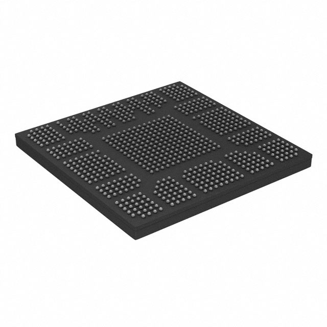
Package
The LFE5UM5G-85F-8BG756I comes in a compact package, which ensures easy integration into electronic systems. The package provides protection against environmental factors such as moisture and dust.
Essence
The essence of the LFE5UM5G-85F-8BG756I lies in its ability to provide a customizable and versatile solution for complex digital logic requirements. It offers a high level of performance and flexibility, making it suitable for a variety of applications.
Packaging/Quantity
The LFE5UM5G-85F-8BG756I is typically packaged individually and is available in various quantities depending on the customer's requirements.
Specifications
- Model: LFE5UM5G-85F-8BG756I
- Logic Elements: 5,000,000
- Speed Grade: 85
- Package Type: BGA
- Package Pins: 756
- Operating Voltage: 1.2V
- Power Consumption: Low
Detailed Pin Configuration
The LFE5UM5G-85F-8BG756I has 756 pins arranged in a Ball Grid Array (BGA) package. The pin configuration includes input/output pins, power supply pins, and configuration pins. A detailed pinout diagram is available in the product datasheet.
Functional Features
- High-speed operation: The LFE5UM5G-85F-8BG756I offers fast processing capabilities, making it suitable for applications that require real-time data processing.
- Flexible design: The FPGA can be reprogrammed to adapt to changing requirements, allowing for easy customization and upgrades.
- Large logic capacity: With 5,000,000 logic elements, the LFE5UM5G-85F-8BG756I can handle complex digital designs efficiently.
- Low power consumption: The FPGA is designed to minimize power consumption, making it energy-efficient and suitable for battery-powered devices.
Advantages and Disadvantages
Advantages
- Versatility: The LFE5UM5G-85F-8BG756I can be used in a wide range of applications due to its flexibility and programmability.
- High performance: The FPGA offers fast processing speeds and large logic capacity, enabling efficient execution of complex algorithms.
- Customizability: The ability to reprogram the FPGA allows for easy customization and adaptation to specific application requirements.
Disadvantages
- Complexity: Working with FPGAs requires specialized knowledge and expertise, which may pose a challenge for some users.
- Cost: FPGAs can be more expensive compared to other integrated circuits, especially for high-capacity models like the LFE5UM5G-85F-8BG756I.
Working Principles
The LFE5UM5G-85F-8BG756I operates based on the principles of digital logic. It consists of configurable logic blocks (CLBs), interconnects, and input/output blocks. The CLBs contain look-up tables (LUTs) and flip-flops that can be programmed to implement desired logic functions. The interconnects provide routing paths between the CLBs, enabling communication and data flow. By configuring the CLBs and interconnects, users can create custom digital circuits within the FPGA.
Detailed Application Field Plans
The LFE5UM5G-85F-8BG756I finds applications in various fields, including:
- Telecommunications: The FPGA can be used for signal processing, protocol implementation, and network optimization in telecommunications systems.
- Aerospace and Defense: It is suitable for radar systems, avionics, and secure communications due to its high performance and reconfigurability.
- Industrial Automation: The FPGA can be utilized for control systems, robotics, and machine vision applications, providing real-time processing capabilities.
- Medical Devices: It can be employed in medical imaging, patient monitoring, and diagnostic equipment, where high-speed data processing is crucial.
- Automotive: The FPGA can be integrated into advanced driver-assistance systems (ADAS), infotainment systems, and engine control units (ECUs) for enhanced functionality.
Detailed and Complete Alternative Models
1.
Liệt kê 10 câu hỏi và câu trả lời thường gặp liên quan đến ứng dụng LFE5UM5G-85F-8BG756I trong giải pháp kỹ thuật
Sure! Here are 10 common questions and answers related to the application of LFE5UM5G-85F-8BG756I in technical solutions:
Q: What is the LFE5UM5G-85F-8BG756I? A: The LFE5UM5G-85F-8BG756I is a field-programmable gate array (FPGA) manufactured by Lattice Semiconductor.
Q: What are the key features of the LFE5UM5G-85F-8BG756I? A: Some key features include 85,000 logic cells, 756 I/O pins, 8GB DDR4 memory, and support for various communication protocols.
Q: What are the typical applications of the LFE5UM5G-85F-8BG756I? A: The LFE5UM5G-85F-8BG756I is commonly used in applications such as high-performance computing, networking, video processing, and industrial automation.
Q: How can I program the LFE5UM5G-85F-8BG756I? A: The LFE5UM5G-85F-8BG756I can be programmed using Lattice Diamond or Lattice Radiant software tools.
Q: What voltage levels does the LFE5UM5G-85F-8BG756I support? A: The LFE5UM5G-85F-8BG756I supports both 1.2V and 3.3V voltage levels.
Q: Can I use the LFE5UM5G-85F-8BG756I in a low-power application? A: Yes, the LFE5UM5G-85F-8BG756I offers power-saving features such as dynamic power management and clock gating to optimize power consumption.
Q: Does the LFE5UM5G-85F-8BG756I support high-speed serial interfaces? A: Yes, the LFE5UM5G-85F-8BG756I supports various high-speed serial interfaces like PCIe, Ethernet, USB, and HDMI.
Q: Can I use the LFE5UM5G-85F-8BG756I for real-time signal processing? A: Absolutely! The LFE5UM5G-85F-8BG756I's high logic capacity and fast performance make it suitable for real-time signal processing applications.
Q: Are there any development boards available for the LFE5UM5G-85F-8BG756I? A: Yes, Lattice Semiconductor provides development boards like the ECP5 Versa Development Kit that are compatible with the LFE5UM5G-85F-8BG756I.
Q: Where can I find technical documentation and support for the LFE5UM5G-85F-8BG756I? A: You can find technical documentation, datasheets, application notes, and support resources on Lattice Semiconductor's official website.