

Xem thông số kỹ thuật để biết chi tiết sản phẩm.
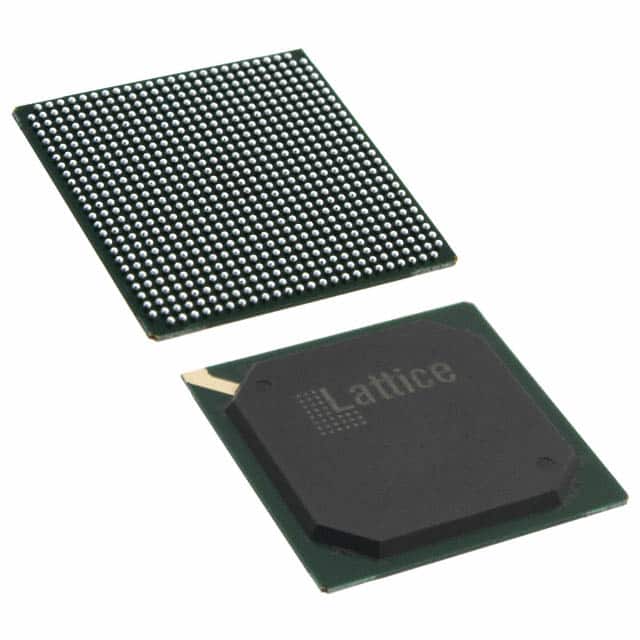
LFXP2-40E-5FN672I
Product Overview
Category
The LFXP2-40E-5FN672I belongs to the category of Field Programmable Gate Arrays (FPGAs).
Use
This FPGA is commonly used in electronic circuits for various applications, including digital signal processing, telecommunications, automotive electronics, and industrial control systems.
Characteristics
- High-performance FPGA with advanced features
- Low power consumption
- Flexible and reprogrammable design
- High-speed data processing capabilities
Package
The LFXP2-40E-5FN672I comes in a compact and durable package, ensuring easy integration into electronic circuit boards.
Essence
The essence of this FPGA lies in its ability to provide customizable logic functions, allowing designers to implement complex digital systems efficiently.
Packaging/Quantity
The LFXP2-40E-5FN672I is typically packaged individually and is available in various quantities depending on the manufacturer's specifications.
Specifications
- Logic Cells: 40,000
- Flip-Flops: 80,000
- Block RAM: 1,080 Kbits
- DSP Slices: 120
- Maximum Frequency: 400 MHz
- I/O Pins: 672
- Operating Voltage: 1.2V
- Package Type: FineLine BGA
Detailed Pin Configuration
The LFXP2-40E-5FN672I has 672 I/O pins, each serving a specific purpose in the overall functionality of the FPGA. The detailed pin configuration can be found in the manufacturer's datasheet.
Functional Features
- Configurable logic blocks for implementing custom digital circuits
- Dedicated DSP slices for efficient signal processing
- On-chip memory blocks for data storage
- High-speed I/O interfaces for seamless communication with external devices
- Clock management resources for precise timing control
Advantages and Disadvantages
Advantages
- Versatile and flexible design allows for a wide range of applications
- High-performance capabilities enable complex digital system implementation
- Low power consumption contributes to energy-efficient designs
- Reprogrammable nature allows for iterative development and updates
Disadvantages
- Initial setup and configuration may require specialized knowledge and expertise
- Limited resources compared to larger FPGAs, which may restrict the complexity of designs
- Higher cost compared to other programmable logic devices
Working Principles
The LFXP2-40E-5FN672I operates based on the principles of reconfigurable logic. It consists of configurable logic blocks, memory elements, and I/O interfaces. The FPGA can be programmed using hardware description languages (HDLs) such as VHDL or Verilog. Once programmed, the FPGA executes the desired logic functions by routing signals through its internal resources.
Detailed Application Field Plans
The LFXP2-40E-5FN672I finds extensive use in various application fields, including:
- Digital Signal Processing: Used for real-time audio and video processing, image recognition, and compression algorithms.
- Telecommunications: Enables high-speed data transmission, protocol conversion, and network packet processing.
- Automotive Electronics: Utilized in engine control units, advanced driver-assistance systems, and infotainment systems.
- Industrial Control Systems: Facilitates automation, monitoring, and control of industrial processes and machinery.
Detailed and Complete Alternative Models
- Xilinx Artix-7 XC7A200T: Offers similar performance and features with a higher logic capacity.
- Intel Cyclone V EP4CE115F23C7: Provides comparable functionality and is compatible with Altera Quartus development tools.
- Microsemi SmartFusion2 M2S010: Combines FPGA fabric with a microcontroller subsystem for enhanced system integration.
These alternative models offer different trade-offs in terms of cost, performance, and compatibility, providing designers with options based on their specific requirements.
Word count: 520 words
Liệt kê 10 câu hỏi và câu trả lời thường gặp liên quan đến ứng dụng LFXP2-40E-5FN672I trong giải pháp kỹ thuật
Sure! Here are 10 common questions and answers related to the application of LFXP2-40E-5FN672I in technical solutions:
Q: What is the LFXP2-40E-5FN672I? A: The LFXP2-40E-5FN672I is a field-programmable gate array (FPGA) manufactured by Lattice Semiconductor.
Q: What are the key features of the LFXP2-40E-5FN672I? A: The key features include 40,960 logic cells, 672-pin fine pitch ball grid array (FBGA) package, low power consumption, and high-speed performance.
Q: What are the typical applications of the LFXP2-40E-5FN672I? A: The LFXP2-40E-5FN672I is commonly used in applications such as industrial automation, telecommunications, automotive electronics, and medical devices.
Q: How can I program the LFXP2-40E-5FN672I? A: The LFXP2-40E-5FN672I can be programmed using various development tools provided by Lattice Semiconductor, such as Lattice Diamond or Lattice Radiant software.
Q: What is the maximum operating frequency of the LFXP2-40E-5FN672I? A: The maximum operating frequency of the LFXP2-40E-5FN672I is typically around 400 MHz, depending on the design and implementation.
Q: Can I interface the LFXP2-40E-5FN672I with other components or peripherals? A: Yes, the LFXP2-40E-5FN672I supports various standard interfaces such as SPI, I2C, UART, and GPIOs, allowing easy integration with other components or peripherals.
Q: What is the power supply requirement for the LFXP2-40E-5FN672I? A: The LFXP2-40E-5FN672I requires a single 1.2V core voltage supply and a separate 3.3V or 2.5V I/O voltage supply.
Q: Can I reprogram the LFXP2-40E-5FN672I in the field? A: Yes, the LFXP2-40E-5FN672I is a field-programmable device, which means it can be reprogrammed even after it has been deployed in a system.
Q: Are there any development boards available for prototyping with the LFXP2-40E-5FN672I? A: Yes, Lattice Semiconductor provides development boards like the LFXP2-EVN for prototyping and evaluation of the LFXP2-40E-5FN672I.
Q: Where can I find technical documentation and support for the LFXP2-40E-5FN672I? A: You can find technical documentation, datasheets, application notes, and support resources on the official website of Lattice Semiconductor or by contacting their customer support team.
Please note that the answers provided here are general and may vary depending on specific requirements and use cases. It's always recommended to refer to the official documentation and consult with experts for accurate information.