

Xem thông số kỹ thuật để biết chi tiết sản phẩm.
LFXP2-8E-6MN132C
Product Overview
Category
The LFXP2-8E-6MN132C belongs to the category of Field-Programmable Gate Arrays (FPGAs).
Use
FPGAs are integrated circuits that can be programmed or reprogrammed after manufacturing. The LFXP2-8E-6MN132C is specifically designed for use in electronic systems where flexibility and customization are required.
Characteristics
- High-performance FPGA with 8,000 Look-Up Tables (LUTs)
- Low power consumption
- Small form factor
- High-speed data processing capabilities
- Configurable I/O pins
- On-chip memory blocks for efficient data storage
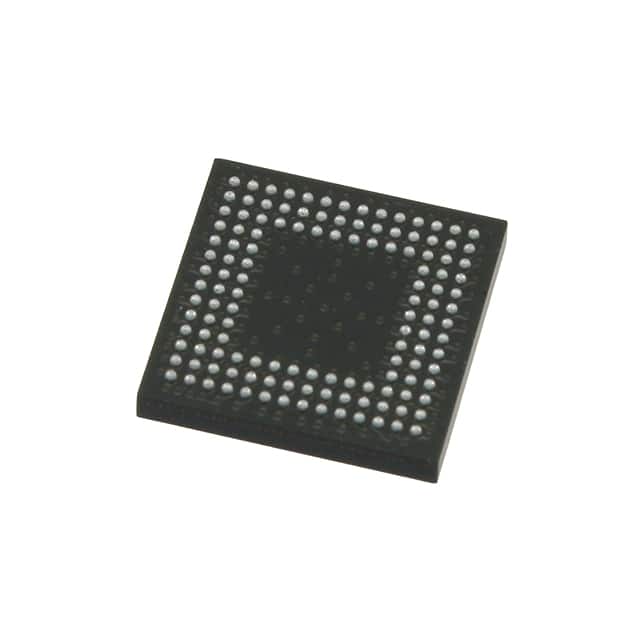
Package
The LFXP2-8E-6MN132C comes in a compact package, suitable for surface-mount technology (SMT) assembly. It is designed to be easily integrated into electronic circuit boards.
Essence
The essence of the LFXP2-8E-6MN132C lies in its ability to provide designers with a versatile and customizable solution for implementing complex digital logic functions.
Packaging/Quantity
The LFXP2-8E-6MN132C is typically packaged in reels or trays, depending on the manufacturer's specifications. The quantity per package may vary, but it is commonly available in quantities of 100 or more.
Specifications
- Logic Elements: 8,000 LUTs
- Flip-Flops: 16,000
- Block RAM: 432 Kbits
- Maximum Frequency: 300 MHz
- I/O Pins: 132
- Operating Voltage: 1.2V
- Package Type: QFN
Detailed Pin Configuration
The LFXP2-8E-6MN132C has 132 I/O pins, each of which can be configured for input or output. The pin configuration is as follows:
(Pin Number) - (Pin Name) 1 - VCCIO 2 - GND 3 - IO0 4 - IO1 5 - IO2 ... 132 - IO131
Functional Features
- High-speed data processing: The LFXP2-8E-6MN132C offers fast data processing capabilities, making it suitable for applications that require real-time performance.
- Configurable I/O pins: The device allows designers to customize the input/output configurations based on their specific requirements.
- On-chip memory blocks: The integrated memory blocks enable efficient data storage and retrieval, reducing the need for external memory components.
- Low power consumption: The FPGA is designed to minimize power consumption, making it suitable for battery-powered devices.
Advantages and Disadvantages
Advantages
- Flexibility: The LFXP2-8E-6MN132C provides designers with the flexibility to implement custom logic functions, allowing for highly tailored solutions.
- Reconfigurability: The FPGA can be reprogrammed multiple times, enabling iterative design improvements without the need for hardware changes.
- Integration: The compact size and surface-mount package make it easy to integrate the FPGA into electronic systems.
Disadvantages
- Complexity: Designing and programming FPGAs requires specialized knowledge and expertise, which may pose a challenge for inexperienced users.
- Cost: FPGAs can be more expensive compared to other integrated circuits due to their versatility and customization capabilities.
Working Principles
The LFXP2-8E-6MN132C operates based on the principles of configurable logic. It consists of an array of Look-Up Tables (LUTs) and flip-flops that can be programmed to implement desired logic functions. The configuration of these elements determines the behavior and functionality of the FPGA.
Detailed Application Field Plans
The LFXP2-8E-6MN132C finds applications in various fields, including:
- Communications: Used in networking equipment, routers, and switches to handle high-speed data processing and protocol conversions.
- Industrial Automation: Employed in control systems for factory automation, robotics, and process control.
- Aerospace and Defense: Utilized in avionics systems, radar signal processing, and secure communication systems.
- Medical Devices: Integrated into medical imaging equipment, patient monitoring systems, and diagnostic devices.
- Automotive: Used in advanced driver-assistance systems (ADAS), infotainment systems, and engine control units.
Detailed and Complete Alternative Models
- LFXP2-5E-6MN132C: Similar to the LFXP2-8E-6MN132C but with 5,000 LUTs instead of 8,000.
- LFXP2-12E-6MN132C: Offers a higher logic capacity with 12,000 LUTs.
- LFXP2-15E-6MN132
Liệt kê 10 câu hỏi và câu trả lời thường gặp liên quan đến ứng dụng LFXP2-8E-6MN132C trong giải pháp kỹ thuật
Sure! Here are 10 common questions and answers related to the application of LFXP2-8E-6MN132C in technical solutions:
Q: What is the LFXP2-8E-6MN132C? A: The LFXP2-8E-6MN132C is a low-power, high-performance field-programmable gate array (FPGA) manufactured by Lattice Semiconductor.
Q: What are the key features of the LFXP2-8E-6MN132C? A: The key features include 8,000 Look-Up Tables (LUTs), 132 user I/O pins, 6 multipliers, low power consumption, and support for various communication protocols.
Q: What are some typical applications of the LFXP2-8E-6MN132C? A: The LFXP2-8E-6MN132C is commonly used in applications such as industrial automation, automotive electronics, consumer electronics, telecommunications, and medical devices.
Q: How can I program the LFXP2-8E-6MN132C? A: The LFXP2-8E-6MN132C can be programmed using Lattice Diamond or Lattice Radiant software tools, which provide a graphical interface for designing and implementing FPGA designs.
Q: What programming languages are supported by the LFXP2-8E-6MN132C? A: The LFXP2-8E-6MN132C supports various hardware description languages (HDLs) such as VHDL and Verilog, which are commonly used for FPGA design.
Q: Can I use the LFXP2-8E-6MN132C for real-time signal processing? A: Yes, the LFXP2-8E-6MN132C is capable of real-time signal processing due to its high-performance capabilities and support for digital signal processing (DSP) functions.
Q: Does the LFXP2-8E-6MN132C have built-in security features? A: Yes, the LFXP2-8E-6MN132C offers security features such as bitstream encryption and authentication to protect the intellectual property stored in the FPGA.
Q: Can I interface the LFXP2-8E-6MN132C with other components or devices? A: Yes, the LFXP2-8E-6MN132C provides multiple I/O pins that can be used to interface with other components or devices, including sensors, actuators, memory, and communication interfaces.
Q: What is the power consumption of the LFXP2-8E-6MN132C? A: The LFXP2-8E-6MN132C is designed to be low-power, consuming minimal energy during operation, making it suitable for battery-powered or energy-efficient applications.
Q: Where can I find additional technical documentation and support for the LFXP2-8E-6MN132C? A: You can find additional technical documentation, datasheets, application notes, and support resources on the official website of Lattice Semiconductor or by contacting their customer support team.
Please note that the answers provided here are general and may vary depending on specific requirements and use cases.