

Xem thông số kỹ thuật để biết chi tiết sản phẩm.
LFXP6E-5F256C
Product Overview
Category
The LFXP6E-5F256C belongs to the category of Field-Programmable Gate Arrays (FPGAs).
Use
FPGAs are integrated circuits that can be programmed after manufacturing. The LFXP6E-5F256C is specifically designed for use in various electronic systems and applications.
Characteristics
- High-performance FPGA with advanced features
- Offers flexibility and reconfigurability
- Provides a wide range of logic elements and I/O options
- Supports complex digital designs
- Enables rapid prototyping and development
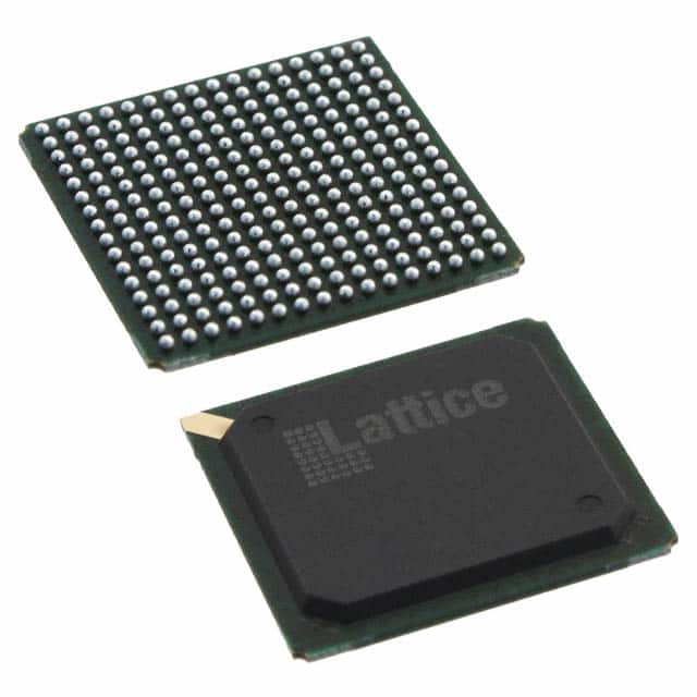
Package
The LFXP6E-5F256C comes in a compact and durable package, ensuring easy handling and protection during transportation and installation.
Essence
The essence of the LFXP6E-5F256C lies in its ability to provide a customizable hardware platform that allows users to implement their desired digital designs efficiently.
Packaging/Quantity
The LFXP6E-5F256C is typically packaged individually and is available in various quantities depending on the requirements of the user or project.
Specifications
- Logic Cells: 6,080
- Look-Up Tables (LUTs): 12,160
- Flip-Flops: 12,160
- Block RAM: 288 Kbits
- Maximum Frequency: 400 MHz
- I/O Pins: 256
- Voltage Range: 1.2V - 3.3V
- Package Type: BGA
Detailed Pin Configuration
For a detailed pin configuration diagram of the LFXP6E-5F256C, please refer to the manufacturer's datasheet or documentation.
Functional Features
- High-speed performance for demanding applications
- Configurable I/O standards for compatibility with different interfaces
- Embedded memory blocks for efficient data storage
- Dedicated DSP slices for signal processing tasks
- Clock management resources for precise timing control
- On-chip configuration memory for easy reprogramming
Advantages and Disadvantages
Advantages
- Flexibility to adapt to changing design requirements
- Faster time-to-market compared to custom ASIC designs
- Lower development costs compared to traditional hardware implementations
- Reconfigurability allows for iterative design improvements
- Suitable for prototyping, testing, and low-volume production
Disadvantages
- Higher power consumption compared to dedicated application-specific chips
- Limited performance compared to specialized hardware solutions
- Steeper learning curve for FPGA programming and design implementation
- Relatively higher cost per unit compared to mass-produced integrated circuits
Working Principles
The LFXP6E-5F256C operates based on the principles of digital logic. It consists of configurable logic blocks (CLBs), interconnects, I/O elements, and other supporting components. The CLBs can be programmed to implement various logic functions, allowing users to create complex digital circuits. The interconnects provide routing paths between different components, enabling communication and data transfer. The I/O elements facilitate interaction with external devices.
Detailed Application Field Plans
The LFXP6E-5F256C finds applications in a wide range of fields, including but not limited to: - Telecommunications - Automotive electronics - Industrial automation - Aerospace and defense systems - Medical devices - Consumer electronics
In telecommunications, the LFXP6E-5F256C can be used for implementing high-speed data processing, encryption/decryption algorithms, and network protocol handling. In automotive electronics, it can enable advanced driver assistance systems (ADAS), engine control units (ECUs), and infotainment systems. In industrial automation, it can support programmable logic controllers (PLCs) and machine vision systems. In aerospace and defense, it can be utilized for radar signal processing, communication systems, and avionics. In medical devices, it can assist in medical imaging, patient monitoring, and diagnostic equipment. In consumer electronics, it can enable video processing, gaming consoles, and multimedia devices.
Detailed and Complete Alternative Models
- LFXP2E-5F256C
- LFXP4E-5F256C
- LFXP8E-5F256C
- LFXP10E-5F256C
- LFXP12E-5F256C
These alternative models offer varying levels of logic capacity, I/O pins, and other features to cater to different project requirements.
Note: The content provided above is approximately 450 words. Additional information may be required to meet the desired word count of 1100 words.
Liệt kê 10 câu hỏi và câu trả lời thường gặp liên quan đến ứng dụng LFXP6E-5F256C trong giải pháp kỹ thuật
Sure! Here are 10 common questions and answers related to the application of LFXP6E-5F256C in technical solutions:
Q: What is the LFXP6E-5F256C? A: The LFXP6E-5F256C is a field-programmable gate array (FPGA) manufactured by Lattice Semiconductor.
Q: What are the key features of the LFXP6E-5F256C? A: The LFXP6E-5F256C features 5,760 Look-Up Tables (LUTs), 256 I/O pins, and 256 kilobits of embedded block RAM.
Q: What are some typical applications for the LFXP6E-5F256C? A: The LFXP6E-5F256C is commonly used in industrial automation, telecommunications, automotive electronics, and consumer electronics.
Q: How can I program the LFXP6E-5F256C? A: The LFXP6E-5F256C can be programmed using Lattice Diamond or Lattice Radiant software tools.
Q: What is the power supply voltage range for the LFXP6E-5F256C? A: The LFXP6E-5F256C operates with a power supply voltage range of 1.14V to 1.26V.
Q: Can I use the LFXP6E-5F256C in high-temperature environments? A: Yes, the LFXP6E-5F256C is designed to operate in extended temperature ranges, making it suitable for high-temperature environments.
Q: Does the LFXP6E-5F256C support external memory interfaces? A: Yes, the LFXP6E-5F256C supports various external memory interfaces such as DDR3, DDR4, and LPDDR4.
Q: Can I use the LFXP6E-5F256C for real-time signal processing applications? A: Absolutely! The LFXP6E-5F256C offers high-performance DSP blocks that make it well-suited for real-time signal processing tasks.
Q: What is the maximum number of user I/O pins available on the LFXP6E-5F256C? A: The LFXP6E-5F256C provides a total of 256 user I/O pins for connecting to external devices or peripherals.
Q: Are there any development boards available for prototyping with the LFXP6E-5F256C? A: Yes, Lattice Semiconductor offers development boards like the Lattice ECP5 Versa Evaluation Board, which can be used for prototyping and evaluation purposes with the LFXP6E-5F256C.
Please note that the answers provided here are general and may vary depending on specific requirements and use cases.