

Xem thông số kỹ thuật để biết chi tiết sản phẩm.
LTC1289CCN#PBF
Product Overview
Category
LTC1289CCN#PBF belongs to the category of integrated circuits (ICs).
Use
This product is commonly used in electronic devices for signal processing and data conversion.
Characteristics
- High precision: LTC1289CCN#PBF offers accurate signal conversion with minimal errors.
- Low power consumption: It operates efficiently, consuming minimal power.
- Wide operating voltage range: This IC can function within a broad range of input voltages.
- Fast conversion speed: It provides rapid signal conversion, enabling real-time data processing.
Package
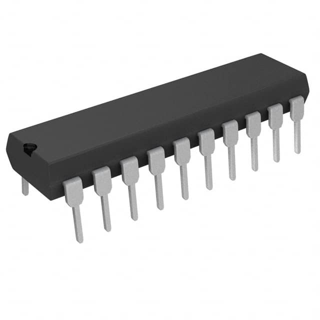
LTC1289CCN#PBF is available in a 16-pin PDIP (Plastic Dual In-line Package) package.
Essence
The essence of LTC1289CCN#PBF lies in its ability to convert analog signals into digital format, facilitating further processing and analysis.
Packaging/Quantity
This product is typically packaged in reels or tubes, with each containing a specific quantity of ICs. The exact quantity may vary depending on the manufacturer's specifications.
Specifications
- Resolution: LTC1289CCN#PBF offers a resolution of 12 bits.
- Input Voltage Range: It supports an input voltage range of ±10V.
- Conversion Rate: The maximum conversion rate is 100 kilosamples per second.
- Operating Temperature Range: This IC can operate within a temperature range of -40°C to +85°C.
- Supply Voltage: It requires a supply voltage between 4.5V and 5.5V.
Detailed Pin Configuration
- VDD: Power supply pin.
- VREF: Reference voltage input pin.
- AGND: Analog ground pin.
- VIN: Analog input pin.
- CS: Chip select input pin.
- SCK: Serial clock input pin.
- SDI: Serial data input pin.
- SDO: Serial data output pin.
- DGND: Digital ground pin.
- DOUT: Digital output pin.
- RD: Read control input pin.
- WR: Write control input pin.
- A0-A3: Address input pins.
- RESET: Reset input pin.
- NC: No connection pin.
- VSS: Negative power supply pin.
Functional Features
- High-resolution conversion: LTC1289CCN#PBF provides accurate and high-resolution analog-to-digital conversion.
- Serial interface: It supports a serial interface for easy integration with microcontrollers and other digital devices.
- Flexible operating modes: This IC offers various operating modes, including continuous conversion and single-shot conversion.
- Low noise performance: It maintains low noise levels during signal conversion, ensuring reliable data acquisition.
Advantages and Disadvantages
Advantages
- High precision conversion ensures accurate data processing.
- Low power consumption extends battery life in portable devices.
- Wide operating voltage range allows compatibility with different power sources.
- Fast conversion speed enables real-time data analysis.
Disadvantages
- Limited resolution compared to higher-end models.
- Requires external components for proper operation.
- Relatively higher cost compared to lower-end alternatives.
Working Principles
LTC1289CCN#PBF operates based on the successive approximation method. It samples the analog input signal and compares it with a reference voltage. By iteratively adjusting the digital code, it converges towards the most accurate representation of the analog input. The converted digital data is then made available through the serial interface for further processing.
Detailed Application Field Plans
LTC1289CCN#PBF finds applications in various fields, including: 1. Industrial automation: Used in data acquisition systems for monitoring and controlling industrial processes. 2. Medical devices: Enables precise measurement and analysis of biological signals. 3. Test and measurement equipment: Provides accurate signal conversion for scientific and engineering instruments. 4. Communication systems: Used in digital communication equipment for signal processing and modulation.
Detailed and Complete Alternative Models
- LTC1290CCN#PBF: Similar to LTC1289CCN#PBF, but with higher resolution (16 bits).
- MAX1241CCSA+: Offers similar functionality with a lower cost.
- ADS1256IPWR: Provides higher resolution (24 bits) at the expense of increased power consumption.
These alternative models offer different trade-offs in terms of resolution, cost, and power consumption, allowing users to choose based on their specific requirements.
Word count: 570 words
Liệt kê 10 câu hỏi và câu trả lời thường gặp liên quan đến ứng dụng LTC1289CCN#PBF trong giải pháp kỹ thuật
Sure! Here are 10 common questions and answers related to the application of LTC1289CCN#PBF in technical solutions:
Q: What is LTC1289CCN#PBF? A: LTC1289CCN#PBF is a specific model number for a digital-to-analog converter (DAC) chip manufactured by Linear Technology Corporation.
Q: What is the purpose of LTC1289CCN#PBF? A: LTC1289CCN#PBF is designed to convert digital signals into analog voltages, making it useful in various applications such as control systems, instrumentation, and communication devices.
Q: What is the resolution of LTC1289CCN#PBF? A: LTC1289CCN#PBF has a resolution of 12 bits, meaning it can represent analog voltages with 4096 discrete levels.
Q: What is the operating voltage range of LTC1289CCN#PBF? A: LTC1289CCN#PBF operates within a voltage range of +5V to +15V.
Q: What is the maximum output current of LTC1289CCN#PBF? A: The maximum output current of LTC1289CCN#PBF is typically around 10 mA.
Q: Does LTC1289CCN#PBF support serial communication interfaces? A: Yes, LTC1289CCN#PBF supports both SPI (Serial Peripheral Interface) and I2C (Inter-Integrated Circuit) communication protocols.
Q: Can LTC1289CCN#PBF be used in low-power applications? A: Yes, LTC1289CCN#PBF has a low power consumption mode that allows it to be used in battery-powered or energy-efficient devices.
Q: What is the temperature range for LTC1289CCN#PBF? A: LTC1289CCN#PBF can operate within a temperature range of -40°C to +85°C.
Q: Does LTC1289CCN#PBF have built-in reference voltage? A: No, LTC1289CCN#PBF requires an external reference voltage source for accurate analog output.
Q: Are there any evaluation boards available for LTC1289CCN#PBF? A: Yes, Linear Technology provides evaluation boards and software tools to help users test and evaluate the performance of LTC1289CCN#PBF in their applications.
Please note that the answers provided here are general and may vary depending on the specific datasheet and application requirements.