

Xem thông số kỹ thuật để biết chi tiết sản phẩm.
LTC1289CCSW#PBF
Product Overview
Category
LTC1289CCSW#PBF belongs to the category of integrated circuits (ICs).
Use
This product is commonly used in electronic devices for signal processing and data conversion.
Characteristics
- High precision: LTC1289CCSW#PBF offers accurate signal conversion with minimal errors.
- Low power consumption: It operates efficiently, consuming minimal power.
- Compact package: The product comes in a small form factor, making it suitable for space-constrained applications.
- Versatile: It can be used in various electronic systems due to its wide compatibility.
Package
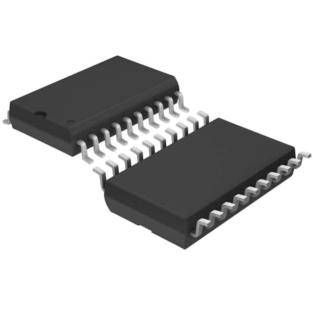
LTC1289CCSW#PBF is packaged in a small outline IC (SOIC) package.
Essence
The essence of LTC1289CCSW#PBF lies in its ability to convert analog signals into digital format and vice versa, enabling seamless communication between different components of an electronic system.
Packaging/Quantity
This product is typically available in reels containing a specific quantity of units. The exact packaging and quantity may vary depending on the supplier.
Specifications
- Resolution: The LTC1289CCSW#PBF offers a resolution of 12 bits.
- Input Voltage Range: It supports input voltage ranging from -5V to +5V.
- Conversion Speed: The product provides a fast conversion speed of up to 1Msps (Mega samples per second).
- Operating Temperature Range: It can operate within a temperature range of -40°C to +85°C.
- Supply Voltage: LTC1289CCSW#PBF requires a supply voltage of +5V.
Detailed Pin Configuration
The LTC1289CCSW#PBF has a total of 20 pins. Here is the detailed pin configuration:
- VDD: Positive supply voltage
- AGND: Analog ground
- REF: Reference voltage input
- IN1: Analog input channel 1
- IN2: Analog input channel 2
- IN3: Analog input channel 3
- IN4: Analog input channel 4
- IN5: Analog input channel 5
- IN6: Analog input channel 6
- IN7: Analog input channel 7
- IN8: Analog input channel 8
- IN9: Analog input channel 9
- IN10: Analog input channel 10
- IN11: Analog input channel 11
- IN12: Analog input channel 12
- CS: Chip select input
- SCK: Serial clock input
- SDI: Serial data input
- SDO: Serial data output
- DGND: Digital ground
Functional Features
- High-resolution conversion: LTC1289CCSW#PBF provides accurate and high-resolution analog-to-digital (ADC) and digital-to-analog (DAC) conversion.
- Serial interface: It supports a serial interface for easy integration with microcontrollers or other digital devices.
- Low noise: The product ensures minimal noise interference during signal conversion, resulting in improved signal quality.
- Flexible power supply: It can operate with a single +5V power supply, simplifying the overall system design.
Advantages and Disadvantages
Advantages
- High precision conversion
- Low power consumption
- Compact form factor
- Versatile compatibility
Disadvantages
- Limited input voltage range (-5V to +5V)
- Requires an external reference voltage for accurate conversion
Working Principles
LTC1289CCSW#PBF operates based on the principle of successive approximation. It utilizes an internal digital-to-analog converter (DAC) and comparator to iteratively approximate the input analog signal. The conversion process involves comparing the DAC output with the input signal and adjusting the DAC value until a close match is achieved. This iterative process continues until the desired resolution is obtained.
Detailed Application Field Plans
LTC1289CCSW#PBF finds applications in various fields, including: 1. Industrial automation: It can be used for precise measurement and control in industrial processes. 2. Medical devices: The product enables accurate data acquisition in medical equipment such as patient monitoring systems. 3. Communication systems: It facilitates signal processing and modulation/demodulation in communication devices. 4. Test and measurement instruments: LTC1289CCSW#PBF is suitable for high-precision measurement instruments like oscilloscopes and data loggers.
Detailed and Complete Alternative Models
- LTC1290CCN#PBF: Similar to LTC1289CCSW#PBF, this model offers 12-bit resolution but comes in a different package (DIP).
- LTC1298CN8#PBF: This alternative model provides 16-bit resolution and operates on a single +5V supply voltage.
- MAX
Liệt kê 10 câu hỏi và câu trả lời thường gặp liên quan đến ứng dụng LTC1289CCSW#PBF trong giải pháp kỹ thuật
Sure! Here are 10 common questions and answers related to the application of LTC1289CCSW#PBF in technical solutions:
Q: What is LTC1289CCSW#PBF? A: LTC1289CCSW#PBF is a specific model number for a digital-to-analog converter (DAC) chip manufactured by Linear Technology Corporation.
Q: What is the purpose of LTC1289CCSW#PBF? A: The LTC1289CCSW#PBF is designed to convert digital signals into analog voltages, making it useful in various applications such as audio systems, instrumentation, and control systems.
Q: What is the resolution of LTC1289CCSW#PBF? A: The LTC1289CCSW#PBF has a resolution of 12 bits, meaning it can represent analog voltages with 4096 discrete levels.
Q: What is the operating voltage range of LTC1289CCSW#PBF? A: The LTC1289CCSW#PBF operates within a voltage range of 2.7V to 5.5V, making it compatible with a wide range of power supply voltages.
Q: How many channels does LTC1289CCSW#PBF have? A: The LTC1289CCSW#PBF is a single-channel DAC, meaning it can generate one analog output voltage at a time.
Q: What is the maximum output voltage range of LTC1289CCSW#PBF? A: The LTC1289CCSW#PBF can generate analog output voltages ranging from 0V to the reference voltage, which is typically equal to the power supply voltage.
Q: Does LTC1289CCSW#PBF support serial communication interfaces? A: Yes, the LTC1289CCSW#PBF supports various serial communication interfaces such as SPI (Serial Peripheral Interface) and I2C (Inter-Integrated Circuit).
Q: Can LTC1289CCSW#PBF be used in low-power applications? A: Yes, the LTC1289CCSW#PBF has a low power consumption mode that can be enabled to reduce its power consumption when not actively converting digital signals.
Q: What is the settling time of LTC1289CCSW#PBF? A: The settling time of LTC1289CCSW#PBF refers to the time it takes for the output voltage to stabilize after a change in the input digital code. It typically ranges from a few microseconds to tens of microseconds.
Q: Are there any evaluation boards or development kits available for LTC1289CCSW#PBF? A: Yes, Linear Technology Corporation provides evaluation boards and development kits specifically designed for LTC1289CCSW#PBF, which can help users quickly prototype and test their applications.
Please note that the answers provided here are general and may vary depending on the specific datasheet and application requirements.