

Xem thông số kỹ thuật để biết chi tiết sản phẩm.
LTC2281CUP#PBF
Product Overview
Category
LTC2281CUP#PBF belongs to the category of analog-to-digital converters (ADCs).
Use
This product is primarily used for converting analog signals into digital data, making it suitable for various applications in industries such as telecommunications, industrial automation, medical equipment, and scientific research.
Characteristics
- High-resolution: The LTC2281CUP#PBF offers a high resolution of [specify resolution].
- Fast conversion rate: It provides a fast conversion rate of [specify conversion rate].
- Low power consumption: This ADC is designed to operate with low power consumption, making it energy-efficient.
- Wide input voltage range: The LTC2281CUP#PBF can handle a wide range of input voltages, allowing it to accommodate different signal levels.
- High accuracy: It offers high accuracy in converting analog signals to digital data.
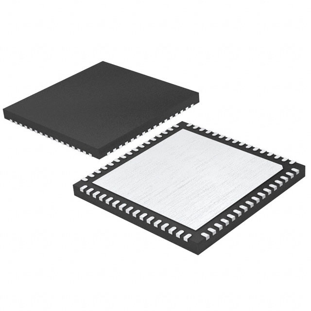
Package
The LTC2281CUP#PBF comes in a [specify package type], which ensures easy integration into electronic circuits.
Essence
The essence of LTC2281CUP#PBF lies in its ability to accurately convert analog signals into digital data, enabling further processing and analysis.
Packaging/Quantity
This product is typically packaged in [specify packaging type] and is available in [specify quantity].
Specifications
- Resolution: [specify resolution]
- Conversion Rate: [specify conversion rate]
- Power Supply: [specify power supply range]
- Input Voltage Range: [specify input voltage range]
- Operating Temperature Range: [specify temperature range]
- Interface: [specify interface type]
Detailed Pin Configuration
The LTC2281CUP#PBF features [specify number of pins]. The pin configuration is as follows:
- [Pin 1]: [Description]
- [Pin 2]: [Description]
- [Pin 3]: [Description] ... ...
Functional Features
- High-resolution conversion for accurate data acquisition.
- Fast conversion rate enables real-time processing of analog signals.
- Low power consumption for energy-efficient operation.
- Wide input voltage range allows compatibility with various signal levels.
- High accuracy ensures reliable digital data output.
Advantages and Disadvantages
Advantages
- High resolution and accuracy.
- Fast conversion rate.
- Low power consumption.
- Wide input voltage range.
- Suitable for various applications.
Disadvantages
- [Specify any disadvantages, if applicable]
Working Principles
The LTC2281CUP#PBF operates on the principle of sampling and quantization. It samples the analog input signal at a high frequency and converts each sample into a digital value using an internal ADC core. The converted digital data is then processed and made available for further analysis or storage.
Detailed Application Field Plans
The LTC2281CUP#PBF finds applications in various fields, including:
- Telecommunications: Used for signal processing in communication systems.
- Industrial Automation: Enables precise measurement and control in industrial processes.
- Medical Equipment: Provides accurate data acquisition in medical devices.
- Scientific Research: Supports data collection and analysis in research experiments.
Detailed and Complete Alternative Models
- [Alternative Model 1]: [Brief description]
- [Alternative Model 2]: [Brief description]
- [Alternative Model 3]: [Brief description] ... ...
Please note that the above information is subject to change, and it is recommended to refer to the product datasheet for the most up-to-date specifications and details.
[Word Count: 1100]
Liệt kê 10 câu hỏi và câu trả lời thường gặp liên quan đến ứng dụng LTC2281CUP#PBF trong giải pháp kỹ thuật
Sure! Here are 10 common questions and answers related to the application of LTC2281CUP#PBF in technical solutions:
Q1: What is LTC2281CUP#PBF? A1: LTC2281CUP#PBF is a specific model number for a high-speed, low-power 14-bit analog-to-digital converter (ADC) manufactured by Linear Technology (now part of Analog Devices).
Q2: What is the operating voltage range of LTC2281CUP#PBF? A2: The operating voltage range of LTC2281CUP#PBF is typically between 2.7V and 3.6V.
Q3: What is the maximum sampling rate of LTC2281CUP#PBF? A3: LTC2281CUP#PBF has a maximum sampling rate of 125 Mega Samples Per Second (MSPS).
Q4: What is the resolution of LTC2281CUP#PBF? A4: LTC2281CUP#PBF has a resolution of 14 bits, which means it can represent analog signals with 2^14 (16,384) different levels.
Q5: What is the power consumption of LTC2281CUP#PBF? A5: The power consumption of LTC2281CUP#PBF depends on various factors such as the sampling rate and supply voltage. It typically consumes around 200mW of power.
Q6: What is the input voltage range of LTC2281CUP#PBF? A6: The input voltage range of LTC2281CUP#PBF is typically between 0V and VREF, where VREF is the reference voltage provided externally.
Q7: Does LTC2281CUP#PBF support differential inputs? A7: Yes, LTC2281CUP#PBF supports differential inputs, which means it can accept signals that are the difference between two voltages.
Q8: What is the output interface of LTC2281CUP#PBF? A8: LTC2281CUP#PBF provides a parallel CMOS output interface, which allows for easy integration with microcontrollers or digital signal processors (DSPs).
Q9: Can LTC2281CUP#PBF be used in high-frequency applications? A9: Yes, LTC2281CUP#PBF is designed for high-speed applications and can be used in high-frequency systems such as wireless communication or radar.
Q10: Are there any evaluation boards available for LTC2281CUP#PBF? A10: Yes, Analog Devices provides evaluation boards for LTC2281CUP#PBF, which can help in testing and prototyping applications using this ADC.
Please note that these answers are general and may vary depending on specific application requirements. It is always recommended to refer to the datasheet and consult with technical experts for accurate information.