

Xem thông số kỹ thuật để biết chi tiết sản phẩm.
LTC2609IGN-1#PBF
Product Overview
Category
The LTC2609IGN-1#PBF belongs to the category of integrated circuits (ICs) specifically designed for digital-to-analog conversion.
Use
This product is primarily used in applications where precise analog voltage generation is required. It provides high-resolution digital-to-analog conversion, making it suitable for various industrial and consumer electronic devices.
Characteristics
- High resolution: The LTC2609IGN-1#PBF offers a resolution of up to 16 bits, ensuring accurate and fine-grained analog voltage output.
- Low power consumption: This IC is designed to operate with low power requirements, making it energy-efficient and suitable for battery-powered devices.
- Wide voltage range: It supports a wide supply voltage range, allowing flexibility in different operating conditions.
- Fast settling time: The LTC2609IGN-1#PBF provides fast settling time, enabling rapid response in dynamic applications.
Package
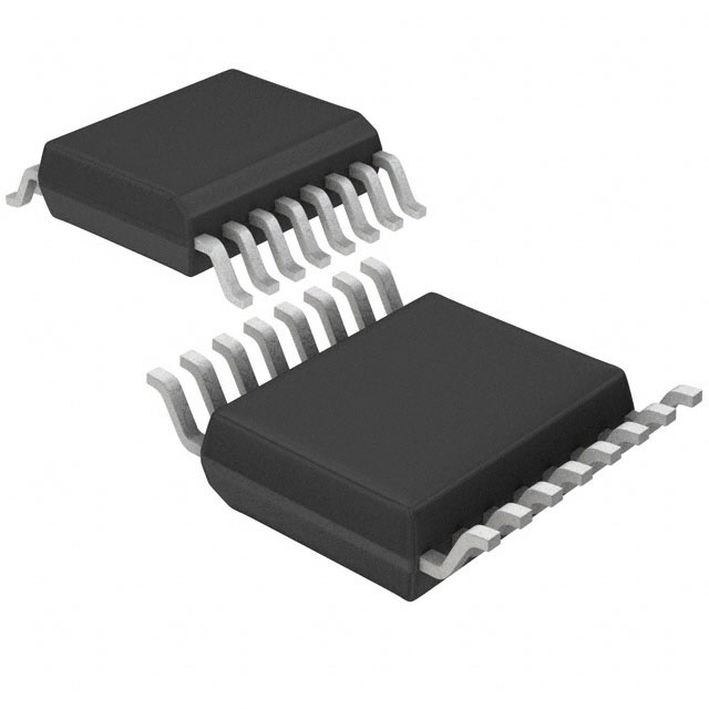
The LTC2609IGN-1#PBF comes in a compact and industry-standard 16-pin SSOP (Shrink Small Outline Package) package. This package ensures easy integration into various circuit designs and facilitates efficient heat dissipation.
Essence
The essence of the LTC2609IGN-1#PBF lies in its ability to convert digital signals into precise analog voltages. This enables accurate control and manipulation of analog components within electronic systems.
Packaging/Quantity
The LTC2609IGN-1#PBF is typically available in tape and reel packaging, which ensures safe transportation and convenient handling during manufacturing processes. The exact quantity per reel may vary depending on the supplier.
Specifications
- Resolution: Up to 16 bits
- Supply Voltage Range: 2.7V to 5.5V
- Operating Temperature Range: -40°C to 85°C
- Output Voltage Range: 0V to VREF
- Digital Interface: I2C-compatible
Detailed Pin Configuration
The LTC2609IGN-1#PBF features a 16-pin SSOP package with the following pin configuration:
- SDA - Serial Data Input
- SCL - Serial Clock Input
- A0 - Address Input Bit 0
- A1 - Address Input Bit 1
- A2 - Address Input Bit 2
- GND - Ground
- REF - Reference Voltage Input
- VDD - Supply Voltage
- VOUT0 - Analog Output Channel 0
- VOUT1 - Analog Output Channel 1
- VOUT2 - Analog Output Channel 2
- VOUT3 - Analog Output Channel 3
- VOUT4 - Analog Output Channel 4
- VOUT5 - Analog Output Channel 5
- VOUT6 - Analog Output Channel 6
- VOUT7 - Analog Output Channel 7
Functional Features
- High-resolution digital-to-analog conversion for precise analog voltage generation.
- Multiple analog output channels for versatile applications.
- I2C-compatible interface for easy integration into digital systems.
- Fast settling time for dynamic applications requiring rapid response.
Advantages and Disadvantages
Advantages
- High resolution enables accurate and fine-grained analog voltage output.
- Low power consumption makes it suitable for energy-efficient devices.
- Wide voltage range allows flexibility in different operating conditions.
- Compact package facilitates easy integration into circuit designs.
Disadvantages
- Limited number of analog output channels may restrict certain applications requiring more outputs.
- Requires an external reference voltage for operation.
Working Principles
The LTC2609IGN-1#PBF operates based on the principle of digital-to-analog conversion. It receives digital input signals through the I2C-compatible interface and converts them into precise analog voltages. These analog voltages can then be utilized to control various analog components within electronic systems.
Detailed Application Field Plans
The LTC2609IGN-1#PBF finds applications in a wide range of fields, including but not limited to: - Industrial automation - Test and measurement equipment - Audio equipment - Medical devices - Automotive electronics - Robotics
In industrial automation, it can be used for precise control of motor speed or position. In audio equipment, it enables accurate volume control and tone adjustment. In medical devices, it can be utilized for precise sensor calibration. The versatility of this IC allows it to be employed in numerous other applications across different industries.
Detailed and Complete Alternative Models
- LTC2607IGN-1#PBF: 16-bit digital-to-analog converter with 8 output channels.
- LTC2611IGN-1#PBF: 14-bit digital-to-analog converter with 8 output channels.
- LTC2630IGN-1#PBF: 12-bit digital-to-analog converter with 8 output channels
Liệt kê 10 câu hỏi và câu trả lời thường gặp liên quan đến ứng dụng LTC2609IGN-1#PBF trong giải pháp kỹ thuật
Sure! Here are 10 common questions and answers related to the application of LTC2609IGN-1#PBF in technical solutions:
Q1: What is the LTC2609IGN-1#PBF? A1: The LTC2609IGN-1#PBF is a digital-to-analog converter (DAC) chip manufactured by Linear Technology (now part of Analog Devices). It is commonly used to convert digital signals into analog voltages.
Q2: What is the resolution of the LTC2609IGN-1#PBF? A2: The LTC2609IGN-1#PBF has a resolution of 16 bits, meaning it can provide 65,536 different output voltage levels.
Q3: What is the operating voltage range of the LTC2609IGN-1#PBF? A3: The LTC2609IGN-1#PBF operates from a single power supply voltage ranging from 2.7V to 5.5V.
Q4: How many channels does the LTC2609IGN-1#PBF have? A4: The LTC2609IGN-1#PBF has 8 independent DAC channels, allowing for simultaneous conversion of multiple digital inputs to analog outputs.
Q5: What is the interface used to communicate with the LTC2609IGN-1#PBF? A5: The LTC2609IGN-1#PBF supports I2C (Inter-Integrated Circuit) communication protocol, making it compatible with a wide range of microcontrollers and other digital devices.
Q6: Can the LTC2609IGN-1#PBF be used in precision applications? A6: Yes, the LTC2609IGN-1#PBF is designed for high accuracy applications, offering low integral nonlinearity (INL) and differential nonlinearity (DNL) specifications.
Q7: What is the output voltage range of the LTC2609IGN-1#PBF? A7: The LTC2609IGN-1#PBF can provide an output voltage range from 0V to VREF, where VREF is the reference voltage supplied to the chip.
Q8: Can the LTC2609IGN-1#PBF operate in a power-down mode? A8: Yes, the LTC2609IGN-1#PBF has a power-down mode that reduces power consumption when the DAC outputs are not required.
Q9: Is the LTC2609IGN-1#PBF suitable for industrial applications? A9: Yes, the LTC2609IGN-1#PBF is designed to operate over an extended temperature range (-40°C to +85°C) and is suitable for various industrial control and automation applications.
Q10: Are there any evaluation boards or development tools available for the LTC2609IGN-1#PBF? A10: Yes, Analog Devices provides evaluation boards and software tools to aid in the development and testing of applications using the LTC2609IGN-1#PBF. These resources can help streamline the design process and ensure optimal performance.
Please note that the answers provided here are general and may vary depending on specific application requirements. It is always recommended to refer to the datasheet and consult with technical experts for accurate and detailed information.