

Xem thông số kỹ thuật để biết chi tiết sản phẩm.
LTC2627IDE-1#PBF
Product Overview
Category
LTC2627IDE-1#PBF belongs to the category of digital-to-analog converters (DACs).
Use
This product is used to convert digital signals into analog voltage outputs.
Characteristics
- High precision and accuracy
- Low power consumption
- Wide operating temperature range
- Small form factor
- Easy integration into various systems
Package
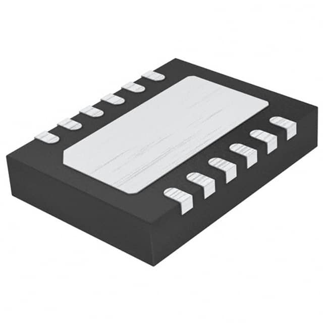
LTC2627IDE-1#PBF comes in a 16-pin plastic dual in-line package (PDIP).
Essence
The essence of LTC2627IDE-1#PBF lies in its ability to provide accurate analog voltage outputs based on digital input signals.
Packaging/Quantity
This product is typically packaged in reels or tubes, with a quantity of 250 units per reel/tube.
Specifications
- Resolution: 12 bits
- Number of Channels: 1
- Output Type: Voltage
- Supply Voltage: 2.7V to 5.5V
- Operating Temperature Range: -40°C to +85°C
- Interface: SPI-compatible
Detailed Pin Configuration
- VDD: Power supply voltage
- GND: Ground reference
- CS: Chip select input
- SCK: Serial clock input
- SDI: Serial data input
- LDAC: Load DAC input
- REF: Reference voltage input
- AGND: Analog ground reference
- OUT: Analog voltage output
- NC: No connection
- NC: No connection
- NC: No connection
- NC: No connection
- NC: No connection
- NC: No connection
- NC: No connection
Functional Features
- High-resolution digital-to-analog conversion
- SPI-compatible interface for easy integration
- Low power consumption for energy-efficient applications
- Internal reference voltage for simplified circuit design
- Output voltage range programmable via digital inputs
Advantages and Disadvantages
Advantages
- High precision and accuracy in analog voltage outputs
- Wide operating temperature range allows for use in various environments
- Small form factor enables space-saving designs
- Easy integration into existing systems due to SPI compatibility
Disadvantages
- Limited to single-channel output
- Requires external reference voltage for operation
Working Principles
LTC2627IDE-1#PBF operates by receiving digital input signals through the SPI interface. These digital signals are then converted into corresponding analog voltages using a high-resolution DAC. The converted analog voltage is then available at the OUT pin for further processing or utilization.
Detailed Application Field Plans
LTC2627IDE-1#PBF finds applications in various fields, including: - Industrial automation - Test and measurement equipment - Audio and video signal processing - Communication systems - Medical devices
Detailed and Complete Alternative Models
Some alternative models to LTC2627IDE-1#PBF include: - LTC2627IDE-2#PBF: 12-bit DAC with dual-channel output - LTC2627IDE-4#PBF: 12-bit DAC with quad-channel output - LTC2627IDE-8#PBF: 12-bit DAC with octal-channel output
These alternative models provide similar functionality but with different channel configurations to suit specific application requirements.
Word count: 446 words
Liệt kê 10 câu hỏi và câu trả lời thường gặp liên quan đến ứng dụng LTC2627IDE-1#PBF trong giải pháp kỹ thuật
Sure! Here are 10 common questions and answers related to the application of LTC2627IDE-1#PBF in technical solutions:
Q1: What is LTC2627IDE-1#PBF? A1: LTC2627IDE-1#PBF is a specific model number for a digital-to-analog converter (DAC) chip manufactured by Linear Technology (now part of Analog Devices). It is used to convert digital signals into analog voltages.
Q2: What is the resolution of LTC2627IDE-1#PBF? A2: The LTC2627IDE-1#PBF has a resolution of 12 bits, meaning it can represent analog voltages with a precision of 1 part in 4096.
Q3: What is the operating voltage range of LTC2627IDE-1#PBF? A3: The operating voltage range of LTC2627IDE-1#PBF is typically between 2.7V and 5.5V.
Q4: How many channels does LTC2627IDE-1#PBF have? A4: LTC2627IDE-1#PBF is a dual-channel DAC, which means it has two independent output channels.
Q5: What is the output voltage range of LTC2627IDE-1#PBF? A5: The output voltage range of LTC2627IDE-1#PBF is determined by the reference voltage applied to its VREF pin. It can be set to any voltage within the operating voltage range.
Q6: What is the interface used to communicate with LTC2627IDE-1#PBF? A6: LTC2627IDE-1#PBF uses an I2C-compatible serial interface for communication with a microcontroller or other digital devices.
Q7: Can LTC2627IDE-1#PBF be used in both single-ended and differential output configurations? A7: Yes, LTC2627IDE-1#PBF can be configured for both single-ended and differential output modes.
Q8: What is the typical settling time of LTC2627IDE-1#PBF? A8: The settling time of LTC2627IDE-1#PBF depends on various factors such as the applied voltage range and load conditions. It typically ranges from a few microseconds to a few milliseconds.
Q9: Can LTC2627IDE-1#PBF operate in a power-down mode? A9: Yes, LTC2627IDE-1#PBF has a power-down mode that reduces its power consumption when not in use.
Q10: Are there any evaluation boards or development kits available for LTC2627IDE-1#PBF? A10: Yes, Analog Devices provides evaluation boards and development kits for LTC2627IDE-1#PBF, which can help in prototyping and testing applications using this DAC chip.
Please note that the answers provided here are general and may vary depending on specific application requirements and datasheet specifications.