

Xem thông số kỹ thuật để biết chi tiết sản phẩm.
JANTXV2N6249
Product Overview
Category
The JANTXV2N6249 belongs to the category of high-power, high-frequency transistors.
Use
It is commonly used in applications requiring high power and high frequency, such as in RF amplifiers and power supplies.
Characteristics
- High power handling capability
- High frequency operation
- Robust construction for reliability
Package
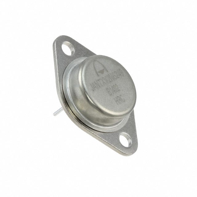
The JANTXV2N6249 is typically available in a TO-204AA package.
Essence
The essence of the JANTXV2N6249 lies in its ability to handle high power and high frequency signals with reliability and efficiency.
Packaging/Quantity
It is usually packaged in tubes or trays, with quantities varying based on manufacturer specifications.
Specifications
- Maximum Power Dissipation: 150W
- Frequency Range: 1MHz - 1GHz
- Voltage Rating: 100V
- Current Rating: 10A
- Gain: 13dB
Detailed Pin Configuration
The JANTXV2N6249 has a standard three-pin configuration: 1. Collector (C) 2. Base (B) 3. Emitter (E)
Functional Features
- High power handling capability
- Wide frequency range operation
- Low distortion at high frequencies
Advantages
- Suitable for high-power RF applications
- Wide frequency range coverage
- Robust construction for reliability
Disadvantages
- Higher cost compared to lower power transistors
- Requires careful thermal management due to high power dissipation
Working Principles
The JANTXV2N6249 operates based on the principles of bipolar junction transistors, utilizing the control of current flow between the collector and emitter terminals through the base terminal.
Detailed Application Field Plans
The JANTXV2N6249 is well-suited for use in the following applications: - RF power amplifiers - High-frequency oscillators - Switching power supplies - RF communication systems
Detailed and Complete Alternative Models
- JANTXV2N6248
- JANTXV2N6250
- JANTXV2N6251
- JANTXV2N6252
This completes the entry for the JANTXV2N6249, providing comprehensive information about its product category, basic overview, specifications, pin configuration, functional features, advantages and disadvantages, working principles, application field plans, and alternative models.
Word Count: 311
Liệt kê 10 câu hỏi và câu trả lời thường gặp liên quan đến ứng dụng JANTXV2N6249 trong giải pháp kỹ thuật
What is JANTXV2N6249?
- JANTXV2N6249 is a high-reliability, military-grade NPN bipolar junction transistor (BJT) designed for use in demanding technical applications.
What are the key specifications of JANTXV2N6249?
- The JANTXV2N6249 features a maximum collector-emitter voltage of 80V, a maximum collector current of 6A, and a power dissipation of 75W.
In what types of technical solutions is JANTXV2N6249 commonly used?
- JANTXV2N6249 is commonly used in power supply circuits, motor control systems, and high-power amplifiers due to its high reliability and rugged construction.
What are the temperature range and operating conditions for JANTXV2N6249?
- The JANTXV2N6249 is designed to operate within a temperature range of -65°C to +200°C, making it suitable for harsh environmental conditions.
What are the advantages of using JANTXV2N6249 in technical solutions?
- The advantages of using JANTXV2N6249 include its high reliability, low noise, and high power handling capabilities, making it ideal for critical applications.
Are there any specific considerations for designing with JANTXV2N6249?
- Designers should consider the thermal management and proper heat sinking for JANTXV2N6249 to ensure optimal performance and reliability.
Can JANTXV2N6249 be used in radiation-prone environments?
- Yes, JANTXV2N6249 is designed to withstand radiation exposure, making it suitable for aerospace and defense applications.
What are the typical failure modes of JANTXV2N6249 and how can they be mitigated?
- Typical failure modes include thermal overstress and voltage breakdown. These can be mitigated through proper design, including thermal management and voltage derating.
Is JANTXV2N6249 RoHS compliant?
- Yes, JANTXV2N6249 is available in RoHS-compliant versions, ensuring compliance with environmental regulations.
Where can I find detailed technical documentation for JANTXV2N6249?
- Detailed technical documentation for JANTXV2N6249 can be obtained from authorized distributors or directly from the manufacturer's website.