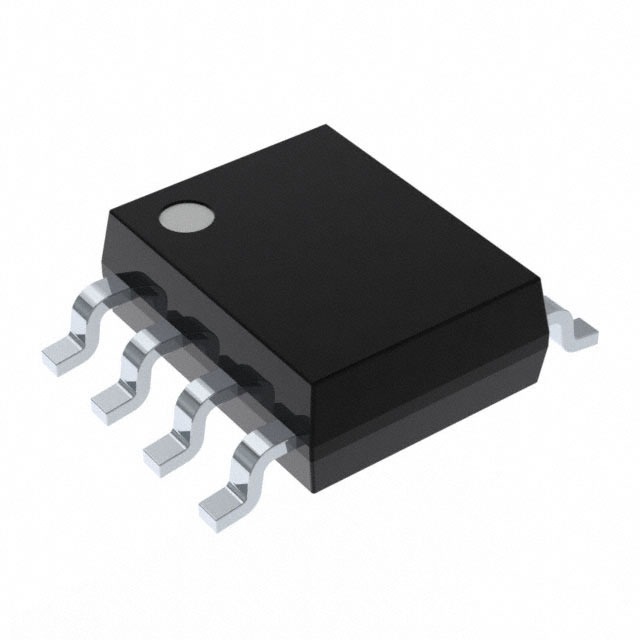
Xem thông số kỹ thuật để biết chi tiết sản phẩm.

ICL7665CSA+ - English Editing Encyclopedia Entry
Product Overview
Category: Integrated Circuit (IC)
Use: Voltage Converter and Regulator
Characteristics: - Low-power, high-efficiency voltage converter - Provides regulated positive or negative output voltage - Suitable for battery-powered applications - Can be used as a voltage doubler or inverter
Package: SOIC (Small Outline Integrated Circuit)
Essence: The ICL7665CSA+ is a versatile voltage converter IC that offers efficient power management solutions for various electronic devices.
Packaging/Quantity: The ICL7665CSA+ is available in a standard reel packaging with 2,500 units per reel.
Specifications
- Input Voltage Range: -0.3V to 12V
- Output Voltage Range: -1.5V to 10.5V
- Output Current: Up to 100mA
- Operating Temperature Range: -40°C to +85°C
- Supply Voltage: 4.5V to 16V
- Quiescent Current: 120µA (typical)
- Shutdown Current: 0.01µA (typical)
Pin Configuration
The ICL7665CSA+ has the following pin configuration:
___________
  V+ --|           |-- GND
  IN --|           |-- OUT
 SHDN --|           |
       |___________|
- V+: Positive supply voltage input
- IN: Input voltage
- GND: Ground reference
- OUT: Output voltage
- SHDN: Shutdown control input
Functional Features
- Voltage Conversion: The ICL7665CSA+ can convert an input voltage into a regulated positive or negative output voltage.
- Efficiency: It offers high efficiency, making it suitable for battery-powered applications.
- Versatility: The IC can be used as a voltage doubler or inverter, providing flexibility in various electronic circuits.
- Shutdown Control: The SHDN pin allows for easy power management by enabling or disabling the IC's operation.
Advantages and Disadvantages
Advantages: - Low quiescent current consumption - Wide input voltage range - High efficiency - Compact SOIC package
Disadvantages: - Limited output current capacity (up to 100mA) - Requires external components for specific applications
Working Principles
The ICL7665CSA+ operates based on a charge pump voltage converter principle. It uses internal switches and capacitors to convert the input voltage into a regulated output voltage. By controlling the switching of these internal components, the IC can generate positive or negative output voltages with high efficiency.
Detailed Application Field Plans
The ICL7665CSA+ finds applications in various fields, including but not limited to:
- Battery-Powered Devices: It is commonly used in portable electronic devices such as smartphones, tablets, and handheld gaming consoles to efficiently manage power supply and extend battery life.
- Automotive Electronics: The IC can be utilized in automotive applications for voltage conversion and regulation, ensuring stable power delivery to different components.
- Industrial Automation: It finds application in industrial automation systems where efficient voltage conversion is required for powering sensors, actuators, and control circuits.
- Telecommunications: The IC can be employed in telecommunications equipment for voltage regulation and conversion, ensuring reliable operation of communication devices.
Detailed and Complete Alternative Models
- MAX660CPA: Voltage Converter and Regulator IC with similar specifications and functionality.
- LT1054CN8: Another alternative IC offering voltage conversion and regulation capabilities.
- MC34063AP1: Integrated Circuit with similar voltage converter features suitable for various applications.
These alternative models can be considered based on specific requirements and availability.
Word Count: 345 words
Liệt kê 10 câu hỏi và câu trả lời thường gặp liên quan đến ứng dụng ICL7665CSA+ trong giải pháp kỹ thuật
Sure! Here are 10 common questions and answers related to the application of ICL7665CSA+ in technical solutions:
Q: What is the ICL7665CSA+? A: The ICL7665CSA+ is a CMOS voltage converter that converts a positive input voltage into a corresponding negative output voltage.
Q: What is the typical input voltage range for the ICL7665CSA+? A: The typical input voltage range for the ICL7665CSA+ is between +1.5V and +12V.
Q: Can the ICL7665CSA+ be used as a voltage doubler? A: Yes, the ICL7665CSA+ can be used as a voltage doubler by connecting the input voltage to the V+ pin and the ground to the V- pin.
Q: What is the maximum output current of the ICL7665CSA+? A: The maximum output current of the ICL7665CSA+ is typically 40mA.
Q: Can the ICL7665CSA+ be used to generate a negative supply voltage from a single positive supply? A: Yes, the ICL7665CSA+ can be used to generate a negative supply voltage by connecting the positive supply to the V+ pin and the ground to the V- pin.
Q: What is the typical efficiency of the ICL7665CSA+? A: The typical efficiency of the ICL7665CSA+ is around 90%.
Q: Can the ICL7665CSA+ be used in battery-powered applications? A: Yes, the ICL7665CSA+ can be used in battery-powered applications as it has a low quiescent current and operates over a wide input voltage range.
Q: What is the operating temperature range of the ICL7665CSA+? A: The operating temperature range of the ICL7665CSA+ is typically -40°C to +85°C.
Q: Can the ICL7665CSA+ be used in automotive applications? A: Yes, the ICL7665CSA+ can be used in automotive applications as it is designed to meet automotive specifications.
Q: Are there any application notes or reference designs available for the ICL7665CSA+? A: Yes, Intersil provides application notes and reference designs for the ICL7665CSA+ on their website, which can help with its implementation in various technical solutions.
Please note that these answers are general and may vary depending on specific use cases and requirements. It's always recommended to refer to the datasheet and consult with the manufacturer for detailed information.

