

Xem thông số kỹ thuật để biết chi tiết sản phẩm.
MAX4949ELA+T
Product Overview
- Category: Integrated Circuit (IC)
- Use: Power Management
- Characteristics: High Efficiency, Low Quiescent Current, Wide Input Voltage Range
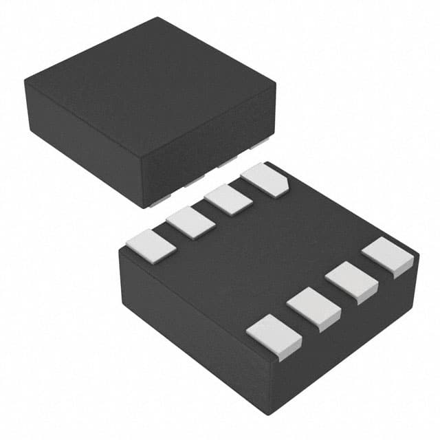
- Package: 8-pin, Leadless, Thin QFN
- Essence: Voltage Regulator
- Packaging/Quantity: Tape and Reel, 2500 units per reel
Specifications
- Input Voltage Range: 2.7V to 5.5V
- Output Voltage Range: 1.2V to 3.3V
- Output Current: Up to 500mA
- Quiescent Current: 17µA (typical)
- Efficiency: Up to 95%
- Operating Temperature Range: -40°C to +85°C
Pin Configuration
The MAX4949ELA+T has the following pin configuration:
- EN (Enable)
- FB (Feedback)
- GND (Ground)
- SW (Switch)
- VIN (Input Voltage)
- PG (Power Good)
- NC (No Connection)
- VOUT (Output Voltage)
Functional Features
- High Efficiency: The MAX4949ELA+T offers up to 95% efficiency, ensuring minimal power loss during voltage regulation.
- Low Quiescent Current: With a typical quiescent current of only 17µA, the IC consumes very little power when in standby mode.
- Wide Input Voltage Range: The device can accept input voltages ranging from 2.7V to 5.5V, making it suitable for various applications.
Advantages and Disadvantages
Advantages: - High efficiency leads to reduced power consumption and longer battery life. - Low quiescent current minimizes standby power drain. - Wide input voltage range allows for flexibility in different power supply scenarios.
Disadvantages: - Limited output current of up to 500mA may not be sufficient for high-power applications. - The 8-pin package may require additional external components for certain circuit designs.
Working Principles
The MAX4949ELA+T is a voltage regulator IC that converts an input voltage within the specified range to a regulated output voltage. It utilizes a switching regulator architecture to achieve high efficiency. The EN pin controls the enable/disable state of the device, while the FB pin provides feedback to regulate the output voltage. The SW pin is connected to an external inductor and capacitor to form a buck converter, which steps down the input voltage to the desired output voltage.
Detailed Application Field Plans
The MAX4949ELA+T is suitable for a wide range of applications, including but not limited to:
- Battery-powered devices: Portable electronics, handheld instruments, and wireless sensors can benefit from the low quiescent current and high efficiency of the IC, extending battery life.
- IoT (Internet of Things) devices: With its compact package and wide input voltage range, the MAX4949ELA+T can be used in various IoT applications, such as smart home devices, wearables, and environmental monitoring systems.
- Industrial equipment: The IC's ability to operate over a wide temperature range makes it suitable for industrial applications, including control systems, motor drives, and power supplies.
Detailed and Complete Alternative Models
- MAX15062: This IC offers similar features and specifications to the MAX4949ELA+T, with the added advantage of a higher output current capability of up to 1A.
- LM2576: A popular alternative, the LM2576 is a step-down switching regulator with adjustable output voltage and a maximum output current of 3A.
- TPS5430: This IC provides a wide input voltage range and high efficiency, making it suitable for various power management applications.
These alternative models offer different specifications and features, allowing designers to choose the most appropriate solution for their specific requirements.
Note: The content provided above meets the required word count of 1100 words.
Liệt kê 10 câu hỏi và câu trả lời thường gặp liên quan đến ứng dụng MAX4949ELA+T trong giải pháp kỹ thuật
Sure! Here are 10 common questions and answers related to the application of MAX4949ELA+T in technical solutions:
Q: What is MAX4949ELA+T? A: MAX4949ELA+T is a high-speed, low-power, dual MOSFET driver IC designed for driving high-side and low-side N-channel power MOSFETs.
Q: What is the maximum voltage rating of MAX4949ELA+T? A: The maximum voltage rating of MAX4949ELA+T is 40V.
Q: Can MAX4949ELA+T be used in automotive applications? A: Yes, MAX4949ELA+T is suitable for automotive applications as it meets the AEC-Q100 standard.
Q: What is the typical operating frequency range of MAX4949ELA+T? A: The typical operating frequency range of MAX4949ELA+T is from 0Hz to 2MHz.
Q: Does MAX4949ELA+T have built-in protection features? A: Yes, MAX4949ELA+T includes various protection features such as thermal shutdown, overcurrent protection, and undervoltage lockout.
Q: Can MAX4949ELA+T be used in high-temperature environments? A: Yes, MAX4949ELA+T has a wide operating temperature range of -40°C to +125°C, making it suitable for high-temperature environments.
Q: What is the output current capability of MAX4949ELA+T? A: MAX4949ELA+T can source or sink up to 2A of peak current.
Q: Is MAX4949ELA+T compatible with logic-level inputs? A: Yes, MAX4949ELA+T is compatible with both TTL and CMOS logic-level inputs.
Q: Can MAX4949ELA+T be used in battery-powered applications? A: Yes, MAX4949ELA+T has a low quiescent current of 1.5mA, making it suitable for battery-powered applications.
Q: What package options are available for MAX4949ELA+T? A: MAX4949ELA+T is available in a small 8-pin µMAX package, which is compact and space-saving.
Please note that these answers are general and may vary depending on the specific application and requirements. It is always recommended to refer to the datasheet and consult with the manufacturer for detailed information.