

Xem thông số kỹ thuật để biết chi tiết sản phẩm.
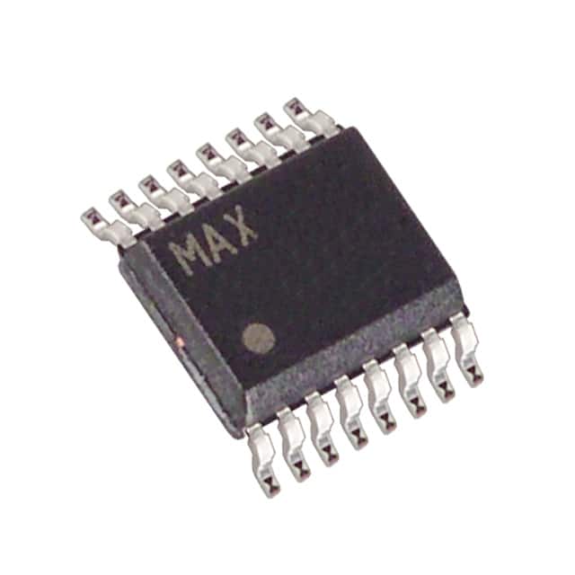
MAX5123BEEE+T
Product Overview
- Category: Integrated Circuit (IC)
- Use: Digital-to-Analog Converter (DAC)
- Characteristics:
- High resolution
- Low power consumption
- Small package size
- Wide operating voltage range
- Package: 16-pin TQFN (Thin Quad Flat No-Lead) package
- Essence: Converts digital signals into analog voltages
- Packaging/Quantity: Tape and reel, 2500 units per reel
Specifications
- Resolution: 12 bits
- Supply Voltage Range: 2.7V to 5.5V
- Operating Temperature Range: -40°C to +85°C
- Output Voltage Range: 0V to Vref
- Reference Voltage Range: 1.25V to Vdd
- Power Consumption: 0.5mW (typical)
Detailed Pin Configuration
The MAX5123BEEE+T has the following pin configuration:
- VDD: Positive supply voltage
- GND: Ground reference
- DIN: Digital input for data
- CS: Chip select input
- SCLK: Serial clock input
- LDAC: Load DAC input
- REF: Reference voltage input
- AGND: Analog ground reference
- OUT: Analog output voltage
- NC: No connection
- NC: No connection
- NC: No connection
- NC: No connection
- NC: No connection
- NC: No connection
- NC: No connection
Functional Features
- High-resolution digital-to-analog conversion
- Low power consumption for energy-efficient operation
- Small package size for space-constrained applications
- Wide operating voltage range for compatibility with various systems
- On-chip reference voltage generator for simplified design
Advantages and Disadvantages
Advantages: - High resolution provides accurate analog output - Low power consumption extends battery life in portable devices - Small package size saves board space - Wide operating voltage range allows for versatile applications - On-chip reference voltage generator simplifies design
Disadvantages: - Limited output voltage range compared to some other DACs - Higher cost compared to lower-resolution DACs
Working Principles
The MAX5123BEEE+T is a digital-to-analog converter that converts digital signals into corresponding analog voltages. It utilizes a 12-bit resolution to provide precise analog output. The device operates within a wide supply voltage range of 2.7V to 5.5V, making it suitable for various electronic systems.
The digital input data is provided through the DIN pin, and the chip select (CS) and serial clock (SCLK) inputs control the conversion process. The load DAC (LDAC) input allows for simultaneous updating of multiple DACs. The reference voltage (REF) input determines the maximum output voltage.
The MAX5123BEEE+T features a built-in reference voltage generator, eliminating the need for an external reference voltage source. This simplifies the design process and reduces component count.
Detailed Application Field Plans
The MAX5123BEEE+T can be used in a wide range of applications, including:
- Audio Systems: Providing high-resolution analog output for audio signal processing.
- Industrial Automation: Generating precise control voltages for industrial equipment.
- Test and Measurement Instruments: Producing accurate analog signals for testing purposes.
- Communication Systems: Converting digital signals into analog voltages for modulation.
- Automotive Electronics: Controlling various functions requiring analog voltage outputs.
Detailed and Complete Alternative Models
- MAX5124BEEE+T: Similar to MAX5123BEEE+T but with 14-bit resolution.
- MAX5125BEEE+T: Similar to MAX5123BEEE+T but with 16-bit resolution.
- MAX5126BEEE+T: Similar to MAX5123BEEE+T but with dual-channel output.
These alternative models offer different resolutions and additional features, providing flexibility for various application requirements.
Word count: 439 words
Liệt kê 10 câu hỏi và câu trả lời thường gặp liên quan đến ứng dụng MAX5123BEEE+T trong giải pháp kỹ thuật
Sure! Here are 10 common questions and answers related to the application of MAX5123BEEE+T in technical solutions:
Q: What is the MAX5123BEEE+T? A: The MAX5123BEEE+T is a digital-to-analog converter (DAC) IC manufactured by Maxim Integrated. It converts digital signals into analog voltages.
Q: What is the voltage range of the MAX5123BEEE+T? A: The MAX5123BEEE+T operates with a voltage range of 2.7V to 5.5V.
Q: How many bits does the MAX5123BEEE+T support? A: The MAX5123BEEE+T is a 12-bit DAC, meaning it can convert digital signals into analog voltages with a resolution of 12 bits.
Q: What is the output voltage range of the MAX5123BEEE+T? A: The MAX5123BEEE+T has an output voltage range of 0V to VREF, where VREF is the reference voltage supplied to the DAC.
Q: Can the MAX5123BEEE+T be used in both single-ended and differential output configurations? A: Yes, the MAX5123BEEE+T can be configured for both single-ended and differential output modes.
Q: What is the typical power consumption of the MAX5123BEEE+T? A: The MAX5123BEEE+T has a typical power consumption of 0.5mW at a 3.3V supply voltage.
Q: Does the MAX5123BEEE+T have any built-in protection features? A: Yes, the MAX5123BEEE+T includes built-in thermal shutdown and short-circuit protection features.
Q: Can the MAX5123BEEE+T be controlled using a microcontroller? A: Yes, the MAX5123BEEE+T can be easily interfaced with a microcontroller using standard digital communication protocols such as I2C or SPI.
Q: What is the temperature range in which the MAX5123BEEE+T can operate? A: The MAX5123BEEE+T has an operating temperature range of -40°C to +85°C.
Q: Are there any evaluation boards or reference designs available for the MAX5123BEEE+T? A: Yes, Maxim Integrated provides evaluation kits and reference designs that can help users quickly prototype and integrate the MAX5123BEEE+T into their technical solutions.
Please note that these answers are general and may vary depending on the specific datasheet and application requirements.