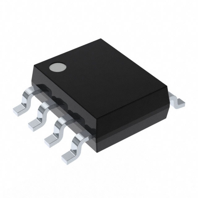
Xem thông số kỹ thuật để biết chi tiết sản phẩm.

MAX541BCSA+ - English Editing Encyclopedia Entry
Product Overview
Category: Integrated Circuits (ICs)
Use: The MAX541BCSA+ is a digital-to-analog converter (DAC) IC that converts digital signals into analog voltage outputs. It is commonly used in various electronic devices and systems where precise analog voltage control is required.
Characteristics: - High resolution: The MAX541BCSA+ offers a resolution of 16 bits, allowing for fine-grained control over the analog output voltage. - Low power consumption: This IC operates at low power levels, making it suitable for battery-powered applications. - Wide voltage range: It supports a wide supply voltage range, typically from 2.7V to 5.5V, enabling compatibility with different power sources. - Small package size: The MAX541BCSA+ comes in a small surface-mount SOIC package, which facilitates easy integration into compact electronic designs. - Digital interface: It features a serial interface that allows for simple communication with microcontrollers or other digital devices.
Package and Quantity: The MAX541BCSA+ is available in a standard SOIC-8 package. Each package contains one IC.
Specifications
- Resolution: 16 bits
- Supply Voltage Range: 2.7V to 5.5V
- Operating Temperature Range: -40°C to +85°C
- Output Voltage Range: 0V to Vref (supply voltage)
- Digital Interface: Serial (SPI-compatible)
Pin Configuration
The MAX541BCSA+ has eight pins arranged as follows:
┌───┬───┐
   │1  8│ VDD
   │2  7│ CS
   │3  6│ SCLK
   │4  5│ DIN
   └───┴───┘
- DIN: Digital Input - Serial data input pin for sending digital control signals.
- CS: Chip Select - Active-low chip select pin used to enable/disable the IC.
- SCLK: Serial Clock - Clock input pin for synchronizing data transfer.
- VDD: Supply Voltage - Positive power supply pin.
Functional Features
- High Precision: The MAX541BCSA+ offers excellent linearity and low integral non-linearity (INL), ensuring accurate analog voltage outputs.
- Fast Settling Time: It has a fast settling time, allowing for rapid changes in the output voltage.
- Power-On Reset: The IC includes a power-on reset circuit that initializes the DAC to a known state upon power-up.
- Low Glitch Energy: The device minimizes glitches during transitions, reducing unwanted noise in the analog output signal.
- Daisy-Chain Capability: Multiple MAX541BCSA+ ICs can be daisy-chained together to achieve higher resolution or control multiple analog outputs simultaneously.
Advantages and Disadvantages
Advantages: - High resolution and accuracy - Low power consumption - Wide voltage range compatibility - Small package size for space-constrained designs - Easy integration with microcontrollers and digital devices
Disadvantages: - Limited output voltage range (0V to Vref) - Requires external voltage reference for precise analog output control
Working Principles
The MAX541BCSA+ operates based on the principle of pulse-width modulation (PWM). It converts digital input signals into proportional analog voltages by adjusting the width of the output pulses. The digital input is processed internally, and the resulting analog voltage is generated at the output pin.
Application Field Plans
The MAX541BCSA+ finds applications in various fields, including: 1. Audio Equipment: It can be used in audio mixers, amplifiers, and equalizers to control volume levels, tone adjustments, and other audio parameters. 2. Industrial Automation: The IC is suitable for industrial control systems that require precise analog voltage control, such as motor speed control, temperature regulation, and process control. 3. Test and Measurement Instruments: It can be utilized in oscilloscopes, function generators, and data acquisition systems to generate accurate analog signals for testing and measurement purposes. 4. Communication Systems: The MAX541BCSA+ can be employed in communication devices like radios, transceivers, and modems to control signal strength, frequency, or modulation.
Alternative Models
- DAC8411E: 16-bit digital-to-analog converter with similar specifications and package size.
- MCP4922-E/P: 12-bit dual-channel DAC with SPI interface and SOIC-8 package.
- AD5667RBRMZ-1: 16-bit DAC with I2C interface and small 10-lead MSOP package.
These alternative models offer comparable functionality and can be considered as substitutes for the MAX541BCSA+ in various applications.
In conclusion, the MAX541BCSA
Liệt kê 10 câu hỏi và câu trả lời thường gặp liên quan đến ứng dụng MAX541BCSA+ trong giải pháp kỹ thuật
Sure! Here are 10 common questions and answers related to the application of MAX541BCSA+ in technical solutions:
Q: What is the MAX541BCSA+? A: The MAX541BCSA+ is a digital-to-analog converter (DAC) IC that converts digital signals into analog voltage outputs.
Q: What is the operating voltage range of MAX541BCSA+? A: The operating voltage range of MAX541BCSA+ is typically between +2.7V and +5.5V.
Q: How many bits of resolution does MAX541BCSA+ have? A: MAX541BCSA+ has 16 bits of resolution, allowing for precise control over the analog output voltage.
Q: Can I use MAX541BCSA+ in battery-powered applications? A: Yes, MAX541BCSA+ can be used in battery-powered applications as it operates within a wide voltage range and has low power consumption.
Q: What is the maximum output current of MAX541BCSA+? A: The maximum output current of MAX541BCSA+ is typically 200µA, which is suitable for driving various loads.
Q: Does MAX541BCSA+ support both unipolar and bipolar output voltage ranges? A: No, MAX541BCSA+ supports only unipolar output voltage ranges, ranging from 0V to VREF.
Q: Can I interface MAX541BCSA+ with microcontrollers or other digital devices? A: Yes, MAX541BCSA+ can be easily interfaced with microcontrollers or other digital devices using standard serial communication protocols like SPI or I2C.
Q: Is there any internal reference voltage available in MAX541BCSA+? A: No, MAX541BCSA+ does not have an internal reference voltage. An external reference voltage must be provided for accurate analog output.
Q: What is the typical settling time of MAX541BCSA+? A: The typical settling time of MAX541BCSA+ is around 10µs, ensuring fast and accurate response to digital input changes.
Q: Can I cascade multiple MAX541BCSA+ devices to achieve higher resolution? A: Yes, you can cascade multiple MAX541BCSA+ devices using their serial interface to achieve higher resolution by effectively increasing the number of bits.

