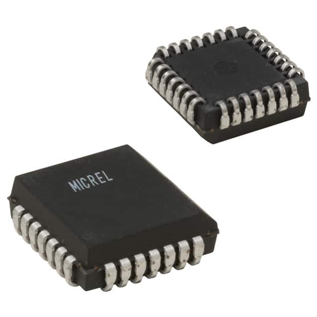
Xem thông số kỹ thuật để biết chi tiết sản phẩm.

SY100E112JI
Product Overview
- Category: Integrated Circuit (IC)
- Use: Digital Logic
- Characteristics: High-speed, ECL-compatible, 8-bit D-type flip-flop
- Package: 28-pin PLCC (Plastic Leaded Chip Carrier)
- Essence: Flip-flop circuit for storing and transferring digital data
- Packaging/Quantity: Available in reels of 250 units
Specifications
- Supply Voltage: -5.2V to -4.5V
- Operating Temperature: -40°C to +85°C
- Propagation Delay: 1.7 ns (typical)
- Output Current: ±24 mA
- Input Voltage: -2.0V to -4.2V
- Output Voltage: -2.0V to -4.2V
Detailed Pin Configuration
The SY100E112JI IC has a total of 28 pins. The pin configuration is as follows:
- CLK (Clock Input)
- D0-D7 (Data Inputs)
- Q0-Q7 (Data Outputs)
- GND (Ground)
- VEE (Negative Power Supply)
- NC (No Connection)
- NC (No Connection)
- NC (No Connection)
- NC (No Connection)
- NC (No Connection)
- NC (No Connection)
- NC (No Connection)
- NC (No Connection)
- NC (No Connection)
- NC (No Connection)
- NC (No Connection)
- NC (No Connection)
- NC (No Connection)
- NC (No Connection)
- NC (No Connection)
- NC (No Connection)
- NC (No Connection)
- NC (No Connection)
- NC (No Connection)
- NC (No Connection)
- NC (No Connection)
- VCC (Positive Power Supply)
- Qn (Complementary Data Output)
Functional Features
- High-speed operation suitable for demanding applications
- Compatible with ECL (Emitter-Coupled Logic) logic levels
- D-type flip-flop functionality for data storage and transfer
- 8-bit width allows handling of larger data sets
- Low propagation delay ensures quick response times
Advantages and Disadvantages
Advantages: - High-speed operation enables efficient data processing - ECL compatibility allows integration with existing systems - Reliable data storage and transfer with the D-type flip-flop - Suitable for applications requiring handling of larger data sets
Disadvantages: - Requires negative power supply (VEE) for operation - Limited availability of alternative models in the market
Working Principles
The SY100E112JI is a high-speed, ECL-compatible 8-bit D-type flip-flop. It operates by storing and transferring digital data using clock signals. The CLK input controls the timing of data transfer, while the D0-D7 inputs receive the data to be stored. The Q0-Q7 outputs provide the stored data, and the Qn output provides the complementary data. The IC requires both positive and negative power supplies (VCC and VEE) for proper operation.
Detailed Application Field Plans
The SY100E112JI IC finds applications in various fields that require high-speed digital logic operations. Some potential application areas include:
- Telecommunications: Used in high-speed data transmission systems.
- Networking: Employed in network switches and routers for efficient data processing.
- Industrial Automation: Integrated into control systems for precise timing and data handling.
- Test and Measurement Equipment: Utilized in instruments requiring fast data capture and analysis.
- Military and Aerospace: Used in mission-critical systems that demand high reliability and speed.
Detailed and Complete Alternative Models
While the SY100E112JI is a reliable and widely used IC, alternative models with similar functionality are limited. However, some alternative options that can be considered include:
- MC10ELT21: 8-bit D-type flip-flop with ECL compatibility.
- SN74F174: 8-bit D-type flip-flop with TTL compatibility.
- CD4013B: Dual D-type flip-flop with CMOS logic levels.
These alternatives may have different specifications and pin configurations, so it is important to carefully review their datasheets before selecting the most suitable option for a specific application.
Word count: 498 words
Liệt kê 10 câu hỏi và câu trả lời thường gặp liên quan đến ứng dụng SY100E112JI trong giải pháp kỹ thuật
Sure! Here are 10 common questions and answers related to the application of SY100E112JI in technical solutions:
Q: What is SY100E112JI? A: SY100E112JI is a specific integrated circuit (IC) chip that belongs to the SY100E112 series. It is commonly used in various technical solutions.
Q: What is the purpose of SY100E112JI? A: The purpose of SY100E112JI is to provide high-speed, low-skew, and low-jitter clock distribution within electronic systems.
Q: What are the key features of SY100E112JI? A: Some key features of SY100E112JI include differential inputs, multiple outputs, low propagation delay, and compatibility with ECL (Emitter-Coupled Logic) logic levels.
Q: In which applications can SY100E112JI be used? A: SY100E112JI can be used in various applications such as telecommunications, data communications, networking equipment, test and measurement instruments, and high-performance computing systems.
Q: How many outputs does SY100E112JI have? A: SY100E112JI has 12 outputs, making it suitable for distributing clock signals to multiple components or subsystems.
Q: What is the operating voltage range of SY100E112JI? A: SY100E112JI operates within a voltage range of -4.2V to -5.7V, making it compatible with ECL logic levels.
Q: Can SY100E112JI operate at high frequencies? A: Yes, SY100E112JI is designed to operate at high frequencies, typically up to several gigahertz.
Q: Is SY100E112JI a surface-mount device (SMD)? A: Yes, SY100E112JI is available in a surface-mount package, which makes it suitable for modern PCB assembly techniques.
Q: Are there any specific design considerations when using SY100E112JI? A: Yes, some design considerations include proper termination of inputs and outputs, careful routing of clock signals to minimize skew, and ensuring adequate power supply decoupling.
Q: Where can I find more information about SY100E112JI? A: You can refer to the datasheet provided by the manufacturer or visit their official website for detailed information on SY100E112JI's specifications, application notes, and recommended usage guidelines.
Please note that the answers provided here are general and may vary depending on the specific requirements and implementation of SY100E112JI in different technical solutions.

