

Xem thông số kỹ thuật để biết chi tiết sản phẩm.
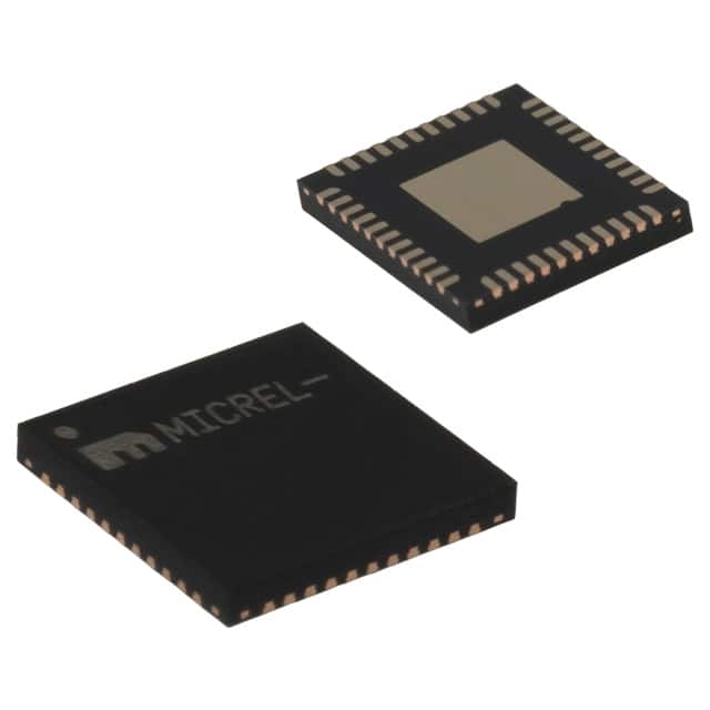
SY89859UMG
Product Overview
- Category: Integrated Circuit (IC)
- Use: Signal Conditioning and Amplification
- Characteristics: High-speed, low-power, small form factor
- Package: Micro Leadframe Package (MLP)
- Essence: Signal conditioning and amplification for high-speed digital communication systems
- Packaging/Quantity: Tape and Reel, 2500 units per reel
Specifications
- Supply Voltage: 3.3V
- Operating Temperature Range: -40°C to +85°C
- Input Voltage Range: 0V to VCC
- Output Voltage Swing: 0V to VCC
- Bandwidth: 1 GHz
- Gain: Adjustable from 0 dB to 20 dB
- Power Consumption: 50 mW
Detailed Pin Configuration
The SY89859UMG IC has the following pin configuration:
- VCC: Power supply voltage input
- GND: Ground reference
- INP: Positive differential input
- INN: Negative differential input
- OUTP: Positive differential output
- OUTN: Negative differential output
- ADJ: Gain adjustment control
- NC: No connection
Functional Features
- High-speed signal conditioning and amplification
- Low power consumption
- Adjustable gain for flexible signal processing
- Differential inputs and outputs for noise rejection
- Wide input and output voltage range
- Small form factor for space-constrained applications
Advantages and Disadvantages
Advantages: - High-speed operation enables efficient signal processing in fast communication systems - Low power consumption reduces energy requirements and heat dissipation - Adjustable gain allows customization for different signal levels - Small form factor saves board space in compact designs
Disadvantages: - Limited bandwidth may not be suitable for ultra-high-frequency applications - Single-ended input/output not supported, limiting compatibility with certain systems
Working Principles
The SY89859UMG is a signal conditioning and amplification IC designed for high-speed digital communication systems. It operates by receiving differential input signals and amplifying them with an adjustable gain. The amplified signals are then provided as differential outputs. The IC is powered by a 3.3V supply voltage and consumes low power while delivering high-speed performance.
Detailed Application Field Plans
The SY89859UMG IC finds applications in various fields, including:
- Telecommunications: Signal conditioning and amplification in high-speed data transmission systems.
- Networking: Enhancing the performance of network switches and routers.
- Test and Measurement: Improving signal integrity in high-frequency test equipment.
- Data Centers: Enabling reliable signal processing in high-speed server and storage systems.
- Industrial Automation: Supporting high-speed communication in industrial control systems.
Detailed and Complete Alternative Models
- SY89858UMG: Similar to SY89859UMG but with a different gain range.
- SY89860UMG: Higher bandwidth version of SY89859UMG for ultra-high-frequency applications.
- SY89861UMG: Lower power consumption variant of SY89859UMG for energy-efficient designs.
These alternative models offer similar functionality with slight variations to cater to specific requirements.
Word count: 320 words
Liệt kê 10 câu hỏi và câu trả lời thường gặp liên quan đến ứng dụng SY89859UMG trong giải pháp kỹ thuật
Sure! Here are 10 common questions and answers related to the application of SY89859UMG in technical solutions:
Q: What is SY89859UMG? A: SY89859UMG is a high-speed, low-power differential receiver commonly used in various technical solutions.
Q: What is the operating voltage range for SY89859UMG? A: The operating voltage range for SY89859UMG is typically between 3.0V and 3.6V.
Q: What is the maximum data rate supported by SY89859UMG? A: SY89859UMG supports a maximum data rate of up to 2.5 Gbps.
Q: Can SY89859UMG be used in both single-ended and differential applications? A: No, SY89859UMG is specifically designed for differential signaling applications.
Q: What is the input common-mode voltage range for SY89859UMG? A: The input common-mode voltage range for SY89859UMG is typically between -0.5V and VCC+0.5V.
Q: Does SY89859UMG have built-in termination resistors? A: No, SY89859UMG does not have built-in termination resistors. External termination resistors are required for proper operation.
Q: Can SY89859UMG be used in high-temperature environments? A: Yes, SY89859UMG is designed to operate in a wide temperature range, typically from -40°C to +85°C.
Q: What is the power supply current consumption of SY89859UMG? A: The power supply current consumption of SY89859UMG is typically around 20 mA.
Q: Is SY89859UMG compatible with LVDS (Low Voltage Differential Signaling) standards? A: Yes, SY89859UMG is fully compatible with LVDS standards.
Q: Can SY89859UMG be used in high-speed communication interfaces like USB or Ethernet? A: Yes, SY89859UMG can be used in various high-speed communication interfaces, including USB and Ethernet, where differential signaling is required.
Please note that the answers provided here are general and may vary depending on specific application requirements and datasheet specifications.