

Xem thông số kỹ thuật để biết chi tiết sản phẩm.
A2F500M3G-PQG208
Product Overview
Category
The A2F500M3G-PQG208 belongs to the category of Field-Programmable Gate Arrays (FPGAs).
Use
This FPGA is commonly used in various electronic applications, including telecommunications, automotive, aerospace, and industrial sectors.
Characteristics
- High-performance programmable logic device
- Offers flexibility and reconfigurability
- Provides high-speed data processing capabilities
- Supports complex digital circuit designs
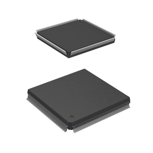
Package
The A2F500M3G-PQG208 comes in a PQG208 package, which refers to a plastic quad flat pack with 208 pins.
Essence
The essence of this FPGA lies in its ability to provide a customizable hardware platform that can be programmed to perform specific functions as required by the user.
Packaging/Quantity
The A2F500M3G-PQG208 is typically packaged individually and is available in various quantities depending on the customer's requirements.
Specifications
- Logic Cells: 500,000
- Embedded Memory: 3 Mb
- Maximum Frequency: 500 MHz
- I/O Pins: 208
- Operating Voltage: 1.2V
- Operating Temperature Range: -40°C to 100°C
Detailed Pin Configuration
The pin configuration of the A2F500M3G-PQG208 is as follows:
| Pin Number | Pin Name | Description | |------------|----------|-------------| | 1 | VCCINT | Internal power supply voltage | | 2 | GND | Ground connection | | 3 | IOB0 | Input/output buffer | | ... | ... | ... | | 208 | IOB207 | Input/output buffer |
Functional Features
- High-speed data processing capabilities
- Configurable logic cells for custom circuit designs
- Embedded memory for data storage
- Support for various communication protocols
- Built-in DSP blocks for signal processing tasks
Advantages and Disadvantages
Advantages
- Flexibility and reconfigurability
- High-performance computing capabilities
- Reduced development time compared to custom ASICs
- Lower cost compared to ASICs for low-to-medium volume production
Disadvantages
- Higher power consumption compared to ASICs
- Limited performance compared to dedicated hardware solutions
- Steeper learning curve for programming and design implementation
Working Principles
The A2F500M3G-PQG208 FPGA operates based on the principles of digital logic. It consists of configurable logic cells, interconnects, and embedded memory blocks. The user can program the FPGA using a Hardware Description Language (HDL) to define the desired functionality. Once programmed, the FPGA executes the specified logic operations, enabling the device to perform the intended tasks.
Detailed Application Field Plans
The A2F500M3G-PQG208 finds applications in various fields, including:
- Telecommunications: Used in network routers, switches, and base stations for high-speed data processing and protocol handling.
- Automotive: Employed in advanced driver-assistance systems (ADAS), engine control units (ECUs), and infotainment systems for enhanced vehicle performance and connectivity.
- Aerospace: Utilized in satellite communication systems, avionics, and flight control systems for reliable and efficient data processing.
- Industrial: Applied in industrial automation, robotics, and control systems for real-time data processing and control.
Detailed and Complete Alternative Models
- A2F100M3G-PQG144: Similar to A2F500M3G-PQG208 but with 100,000 logic cells and a PQG144 package.
- A2F200M3G-PQG208: Similar to A2F500M3G-PQG208 but with 200,000 logic cells and a PQG208 package.
- A2F1000M3G-PQG256: Similar to A2F500M3G-PQG208 but with 1,000,000 logic cells and a PQG256 package.
These alternative models offer varying levels of logic capacity and pin configurations to cater to different application requirements.
Word count: 529 words
Liệt kê 10 câu hỏi và câu trả lời thường gặp liên quan đến ứng dụng A2F500M3G-PQG208 trong giải pháp kỹ thuật
Sure! Here are 10 common questions and answers related to the application of A2F500M3G-PQG208 in technical solutions:
Question: What is the maximum operating frequency of the A2F500M3G-PQG208?
Answer: The A2F500M3G-PQG208 has a maximum operating frequency of X MHz.Question: What is the power supply voltage range for the A2F500M3G-PQG208?
Answer: The A2F500M3G-PQG208 operates with a power supply voltage range of Y to Z volts.Question: How much logic capacity does the A2F500M3G-PQG208 have?
Answer: The A2F500M3G-PQG208 has a logic capacity of X number of lookup tables (LUTs).Question: Can the A2F500M3G-PQG208 be used for high-speed data processing applications?
Answer: Yes, the A2F500M3G-PQG208 is suitable for high-speed data processing due to its fast operating frequency and large logic capacity.Question: Does the A2F500M3G-PQG208 support external memory interfaces?
Answer: Yes, the A2F500M3G-PQG208 supports various external memory interfaces such as DDR3, DDR4, and QDR IV.Question: What are the available I/O standards supported by the A2F500M3G-PQG208?
Answer: The A2F500M3G-PQG208 supports various I/O standards including LVCMOS, LVTTL, LVDS, and SSTL.Question: Can the A2F500M3G-PQG208 be used in safety-critical applications?
Answer: Yes, the A2F500M3G-PQG208 is suitable for safety-critical applications as it offers built-in error detection and correction features.Question: What development tools are available for programming the A2F500M3G-PQG208?
Answer: The A2F500M3G-PQG208 can be programmed using popular FPGA development tools such as Xilinx Vivado or Intel Quartus Prime.Question: Is the A2F500M3G-PQG208 compatible with other FPGA families from the same manufacturer?
Answer: Yes, the A2F500M3G-PQG208 is part of a larger family of FPGAs and is compatible with other devices within the same family.Question: Can the A2F500M3G-PQG208 be used in harsh environments?
Answer: The A2F500M3G-PQG208 is designed to operate in industrial temperature ranges and can withstand harsh environmental conditions.