

Xem thông số kỹ thuật để biết chi tiết sản phẩm.
A40MX02-1PQ100I
Product Overview
Category
The A40MX02-1PQ100I belongs to the category of programmable logic devices (PLDs).
Use
This device is primarily used for digital circuit design and implementation. It offers a flexible and customizable solution for various applications.
Characteristics
- Programmable: The A40MX02-1PQ100I can be programmed to perform specific functions based on user requirements.
- High Integration: It integrates multiple logic gates, flip-flops, and other components into a single chip.
- Reconfigurable: The device can be reprogrammed multiple times, allowing for design modifications and updates.
- Low Power Consumption: It operates efficiently with low power consumption.
- Fast Operation: The A40MX02-1PQ100I provides high-speed performance for time-critical applications.
Package and Quantity
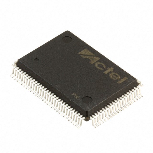
The A40MX02-1PQ100I is available in a PQ100 package, which refers to a plastic quad flat pack with 100 pins. Each package contains one unit of the device.
Specifications
- Logic Cells: 2,000
- Maximum Frequency: 100 MHz
- Operating Voltage: 3.3V
- I/O Pins: 100
- Programmable Gates: AND, OR, XOR, etc.
- Flip-Flops: D-type, JK-type, etc.
- Memory Elements: SRAM, ROM, etc.
- Clock Management: PLL, DLL, etc.
- Configuration Memory: Flash, EEPROM, etc.
Pin Configuration
The A40MX02-1PQ100I has a total of 100 pins, each serving a specific purpose. Here is a brief overview of some key pin functionalities:
- VCC: Power supply pin (+3.3V)
- GND: Ground pin (0V reference)
- I/O Pins: Bidirectional pins for input/output operations
- Clock Pins: Input pins for clock signals
- Configuration Pins: Pins for programming and configuring the device
For a detailed pin configuration diagram, please refer to the manufacturer's datasheet.
Functional Features
- Flexible Logic Design: The A40MX02-1PQ100I allows users to implement complex logic functions using programmable gates and memory elements.
- Reconfigurability: The device can be reprogrammed multiple times, enabling design changes without requiring hardware modifications.
- High-Speed Operation: With a maximum frequency of 100 MHz, it offers fast processing capabilities for time-critical applications.
- Integration: The A40MX02-1PQ100I integrates various components into a single chip, reducing the need for external circuitry.
- Low Power Consumption: It operates efficiently with low power requirements, making it suitable for battery-powered devices.
Advantages and Disadvantages
Advantages
- Versatility: The A40MX02-1PQ100I can be used in a wide range of applications due to its programmable nature.
- Cost-Effective: By eliminating the need for custom-designed circuits, it reduces development costs.
- Time-Saving: The reprogrammability feature allows for faster prototyping and design iterations.
- Compact Design: Its integration capabilities help reduce the overall size of the circuit.
Disadvantages
- Limited Resources: The device has a finite number of logic cells and I/O pins, which may restrict the complexity of designs.
- Learning Curve: Utilizing PLDs requires knowledge of hardware description languages and digital design concepts.
- Non-Volatile Memory: Unlike some other PLDs, the A40MX02-1PQ100I does not have built-in non-volatile memory, requiring external storage for configuration data.
Working Principles
The A40MX02-1PQ100I operates based on the principles of programmable logic. It consists of configurable logic blocks (CLBs), interconnect resources, and input/output blocks (IOBs). The CLBs contain lookup tables (LUTs) that can be programmed to implement specific logic functions. The interconnect resources facilitate the routing of signals between different components, while the IOBs provide interfaces for external connections.
During operation, the device is configured by loading a bitstream into its configuration memory. This bitstream defines the desired logic functions and interconnections within the device. Once configured, the A40MX02-1PQ100I performs the specified operations based on the input signals received.
Application Field Plans
The A40MX02-1PQ100I finds applications in various fields, including:
- Embedded Systems: It can be used to implement control and communication functions in embedded systems.
- Digital Signal Processing: The device enables the implementation of signal processing algorithms in real-time applications.
- Industrial Automation: It can be utilized for controlling and monitoring processes in industrial automation systems.
- Communication Systems: The A40MX02
Liệt kê 10 câu hỏi và câu trả lời thường gặp liên quan đến ứng dụng A40MX02-1PQ100I trong giải pháp kỹ thuật
Sure! Here are 10 common questions and answers related to the application of A40MX02-1PQ100I in technical solutions:
1. What is A40MX02-1PQ100I? A40MX02-1PQ100I is a specific model of field-programmable gate array (FPGA) manufactured by Microsemi Corporation.
2. What are the key features of A40MX02-1PQ100I? Some key features of A40MX02-1PQ100I include 40,000 usable gates, 2,048 macrocells, 64 I/O pins, and a maximum operating frequency of 200 MHz.
3. What are the typical applications of A40MX02-1PQ100I? A40MX02-1PQ100I is commonly used in various technical solutions such as digital signal processing, telecommunications, industrial automation, and embedded systems.
4. How can A40MX02-1PQ100I be programmed? A40MX02-1PQ100I can be programmed using hardware description languages (HDLs) like VHDL or Verilog, which describe the desired functionality of the FPGA.
5. Can A40MX02-1PQ100I be reprogrammed after initial programming? Yes, A40MX02-1PQ100I is a reprogrammable FPGA, allowing for multiple iterations of programming and design changes.
6. What development tools are available for working with A40MX02-1PQ100I? Microsemi provides development tools like Libero SoC Design Suite, which includes software for designing, simulating, and programming A40MX02-1PQ100I.
7. What is the power consumption of A40MX02-1PQ100I? The power consumption of A40MX02-1PQ100I depends on the specific design and usage, but it typically operates at low power levels.
8. Can A40MX02-1PQ100I interface with other components or devices? Yes, A40MX02-1PQ100I can interface with various components and devices through its I/O pins, allowing for communication and integration within a larger system.
9. Are there any limitations or considerations when using A40MX02-1PQ100I? Some considerations include the limited number of usable gates and macrocells, as well as the maximum operating frequency. It's important to ensure that the design fits within these constraints.
10. Where can I find more information about A40MX02-1PQ100I? You can find more detailed information about A40MX02-1PQ100I in the datasheet provided by Microsemi Corporation. Additionally, their website and online forums may have further resources and support available.