

Xem thông số kỹ thuật để biết chi tiết sản phẩm.
A54SX72A-FGG256
Product Overview
Category
The A54SX72A-FGG256 belongs to the category of Field-Programmable Gate Arrays (FPGAs).
Use
This FPGA is designed for use in various electronic systems that require high-performance digital logic circuits.
Characteristics
- High-density integration: The A54SX72A-FGG256 offers a large number of programmable logic cells, allowing for complex designs.
- Flexible configuration: It can be reprogrammed multiple times, making it suitable for prototyping and iterative development.
- Fast operation: The FPGA operates at high clock frequencies, enabling rapid data processing.
- Low power consumption: It is designed to minimize power usage, making it energy-efficient.
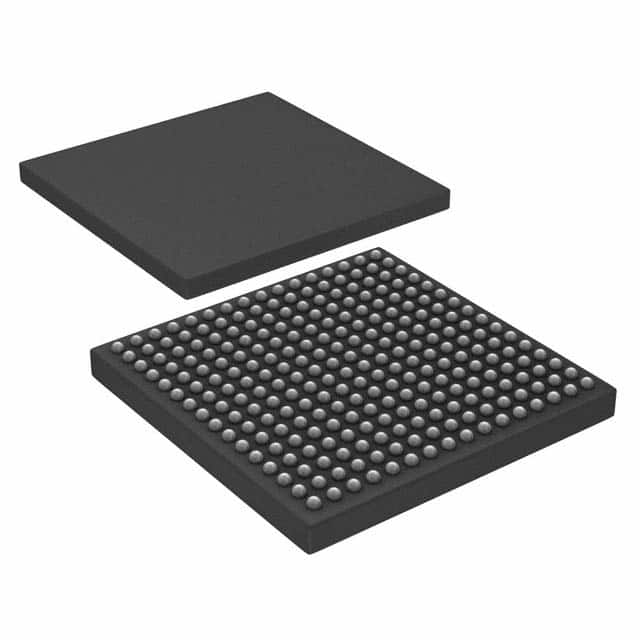
Package
The A54SX72A-FGG256 comes in a compact package, which ensures easy integration into electronic systems. The package type is Fine-Pitch Ball Grid Array (FBGA).
Essence
The essence of this FPGA lies in its ability to provide a customizable digital logic circuitry solution, offering flexibility and high performance.
Packaging/Quantity
Each package of the A54SX72A-FGG256 contains one FPGA unit.
Specifications
- Logic Cells: 54,000
- Maximum Frequency: 500 MHz
- Embedded Memory: 2,000 Kbits
- I/O Pins: 256
- Operating Voltage: 1.2V
- Package Dimensions: 17mm x 17mm
Detailed Pin Configuration
The A54SX72A-FGG256 has 256 I/O pins, each serving a specific purpose in the overall functionality of the FPGA. For a detailed pin configuration diagram, please refer to the manufacturer's datasheet.
Functional Features
- Programmability: The FPGA can be programmed to implement any desired digital logic function.
- Reconfigurability: It allows for dynamic reconfiguration, enabling changes to the circuitry without requiring hardware modifications.
- High-speed Interfaces: The FPGA supports various high-speed interfaces such as DDR, PCIe, and Ethernet, facilitating seamless integration with other components.
- Embedded Memory: It includes a significant amount of embedded memory, which can be utilized for data storage or implementing complex algorithms.
Advantages and Disadvantages
Advantages
- Flexibility: The A54SX72A-FGG256 offers immense flexibility in designing digital logic circuits, allowing for customization according to specific requirements.
- Rapid Prototyping: Its reprogrammable nature enables quick prototyping and iterative development, reducing time-to-market.
- High Performance: With a large number of logic cells and high clock frequencies, this FPGA delivers excellent performance for demanding applications.
Disadvantages
- Complexity: Utilizing FPGAs requires expertise in digital design and programming, making it less accessible for beginners.
- Cost: FPGAs tend to be more expensive compared to other integrated circuits due to their advanced features and programmability.
Working Principles
The A54SX72A-FGG256 operates based on the principles of configurable logic. It consists of an array of programmable logic cells interconnected through configurable routing resources. These logic cells can be programmed to implement various digital functions by configuring the interconnections between them. The configuration is stored in internal memory elements, allowing for dynamic reconfiguration when required.
Detailed Application Field Plans
The A54SX72A-FGG256 finds applications in various fields, including but not limited to: - Telecommunications: Used in base stations, network switches, and routers for high-speed data processing. - Aerospace and Defense: Employed in radar systems, avionics, and military communication equipment for their high-performance computing capabilities. - Industrial Automation: Utilized in control systems, robotics, and machine vision applications for real-time data processing and control. - Medical Devices: Integrated into medical imaging equipment, patient monitoring systems, and laboratory instruments for data acquisition and processing.
Detailed and Complete Alternative Models
- A54SX16A-FGG256: A lower-density version of the same FPGA series, suitable for applications with less demanding requirements.
- A54SX144A-FGG256: A higher-density variant offering more logic cells and I/O pins, ideal for complex designs requiring extensive resources.
- A54SX32A-FGG256: A mid-range option providing a balance between density and cost-effectiveness, suitable for a wide range of applications.
Please note that the above alternative models are part of the same FPGA series and share similar characteristics, but differ in terms of capacity and pin count.
Word count: 623 words
Liệt kê 10 câu hỏi và câu trả lời thường gặp liên quan đến ứng dụng A54SX72A-FGG256 trong giải pháp kỹ thuật
Sure! Here are 10 common questions and answers related to the application of A54SX72A-FGG256 in technical solutions:
Q: What is the A54SX72A-FGG256? A: The A54SX72A-FGG256 is a specific model of field-programmable gate array (FPGA) manufactured by Microsemi.
Q: What are the key features of the A54SX72A-FGG256? A: Some key features include 54,000 logic cells, 72,000 flip-flops, 288 embedded multipliers, and 4.5 Mb of embedded memory.
Q: What are the typical applications of the A54SX72A-FGG256? A: The A54SX72A-FGG256 is commonly used in various technical solutions such as telecommunications, industrial automation, aerospace, and defense systems.
Q: How can I program the A54SX72A-FGG256? A: The A54SX72A-FGG256 can be programmed using hardware description languages (HDLs) like VHDL or Verilog, and then synthesized and implemented using appropriate software tools.
Q: Can the A54SX72A-FGG256 be reprogrammed after deployment? A: Yes, the A54SX72A-FGG256 is a reprogrammable FPGA, allowing for flexibility and updates to the design even after deployment.
Q: What is the power consumption of the A54SX72A-FGG256? A: The power consumption of the A54SX72A-FGG256 varies depending on the design and operating conditions, but it typically falls within a certain range specified in the datasheet.
Q: Does the A54SX72A-FGG256 support high-speed interfaces? A: Yes, the A54SX72A-FGG256 supports various high-speed interfaces such as DDR3/DDR4 memory controllers, PCIe, Ethernet, and USB.
Q: Can I use the A54SX72A-FGG256 for real-time signal processing applications? A: Absolutely! The A54SX72A-FGG256's embedded multipliers and dedicated DSP blocks make it well-suited for real-time signal processing tasks.
Q: Are there any development boards available for the A54SX72A-FGG256? A: Yes, Microsemi offers development boards specifically designed for the A54SX72A-FGG256, which provide a convenient platform for prototyping and testing.
Q: Where can I find technical documentation and support for the A54SX72A-FGG256? A: You can find technical documentation, datasheets, application notes, and support resources on Microsemi's official website or by contacting their customer support team.