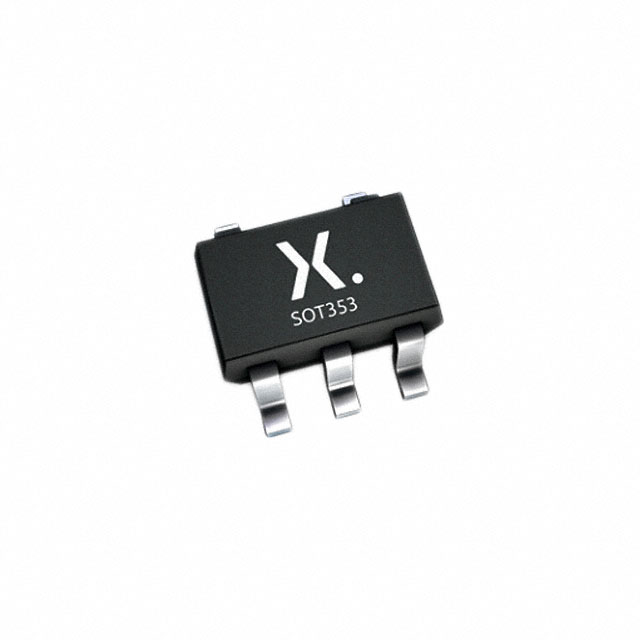
Xem thông số kỹ thuật để biết chi tiết sản phẩm.

74AHC1G125GW,125
Basic Information Overview
- Category: Integrated Circuit (IC)
- Use: Buffer/Driver
- Characteristics: Single Gate, Non-Inverting, Tri-State Output
- Package: SOT753 (SC-70)
- Essence: High-Speed CMOS Logic
- Packaging/Quantity: Tape and Reel, 3000 pieces per reel
Specifications
- Supply Voltage Range: 2.0V to 5.5V
- Input Voltage Range: 0V to VCC
- Output Voltage Range: 0V to VCC
- Maximum Operating Frequency: 400 MHz
- Propagation Delay: 4.5 ns (typical)
- Output Drive Capability: ±24 mA
Detailed Pin Configuration
The 74AHC1G125GW,125 IC has a total of 5 pins: 1. GND (Ground) 2. A (Input) 3. OE (Output Enable) 4. Y (Output) 5. VCC (Supply Voltage)
Functional Features
- Single gate buffer/driver with tri-state output
- Non-inverting logic function
- High-speed operation suitable for various applications
- Wide supply voltage range allows compatibility with different systems
- Low power consumption
- Schmitt-trigger input for noise immunity
Advantages
- Small package size enables space-saving designs
- Tri-state output allows multiple devices to share a common bus
- High-speed operation enhances system performance
- Wide supply voltage range provides flexibility in different applications
- Low power consumption helps prolong battery life in portable devices
Disadvantages
- Limited output drive capability may not be suitable for high-current applications
- Single gate configuration restricts the number of inputs/outputs available
Working Principles
The 74AHC1G125GW,125 is based on high-speed CMOS technology, which combines the advantages of both CMOS and TTL logic families. It operates by amplifying and buffering the input signal to provide a clean and reliable output signal. The tri-state output feature allows the device to be effectively disconnected from the bus when not in use.
Detailed Application Field Plans
The 74AHC1G125GW,125 is commonly used in various applications, including: - Communication systems - Computer peripherals - Industrial automation - Consumer electronics - Automotive electronics
Detailed and Complete Alternative Models
Some alternative models that can be considered as replacements for the 74AHC1G125GW,125 are: - SN74LVC1G125DBVR (Texas Instruments) - MC74VHC1GT125DF2G (ON Semiconductor) - NC7SZ125P5X (Fairchild Semiconductor)
Note: These alternative models may have slightly different specifications and pin configurations, so it is important to refer to their respective datasheets for detailed information.
This entry provides an overview of the 74AHC1G125GW,125 IC, including its basic information, specifications, pin configuration, functional features, advantages, disadvantages, working principles, application field plans, and alternative models.
Liệt kê 10 câu hỏi và câu trả lời thường gặp liên quan đến ứng dụng 74AHC1G125GW,125 trong giải pháp kỹ thuật
Sure! Here are 10 common questions and answers related to the application of 74AHC1G125GW,125 in technical solutions:
Q1: What is the function of the 74AHC1G125GW,125? A1: The 74AHC1G125GW,125 is a single bus buffer gate with 3-state output. It is used to control the flow of data between different parts of a circuit.
Q2: What is the operating voltage range for the 74AHC1G125GW,125? A2: The operating voltage range for the 74AHC1G125GW,125 is typically between 2.0V and 5.5V.
Q3: How many inputs does the 74AHC1G125GW,125 have? A3: The 74AHC1G125GW,125 has one input.
Q4: How many outputs does the 74AHC1G125GW,125 have? A4: The 74AHC1G125GW,125 has one output.
Q5: What is the maximum output current of the 74AHC1G125GW,125? A5: The maximum output current of the 74AHC1G125GW,125 is typically 8mA.
Q6: Can the 74AHC1G125GW,125 be used in high-speed applications? A6: Yes, the 74AHC1G125GW,125 is designed for high-speed operation and can be used in such applications.
Q7: Does the 74AHC1G125GW,125 have internal pull-up or pull-down resistors? A7: No, the 74AHC1G125GW,125 does not have internal pull-up or pull-down resistors.
Q8: Can the 74AHC1G125GW,125 be used in both digital and analog circuits? A8: The 74AHC1G125GW,125 is primarily designed for digital applications, but it can also be used in some analog circuits.
Q9: What is the maximum propagation delay of the 74AHC1G125GW,125? A9: The maximum propagation delay of the 74AHC1G125GW,125 is typically 5.5ns.
Q10: Is the 74AHC1G125GW,125 available in different package options? A10: Yes, the 74AHC1G125GW,125 is available in various package options, such as SOT353 and XSON6.

