

Xem thông số kỹ thuật để biết chi tiết sản phẩm.
74AHCT2G125GD,125
Basic Information Overview
- Category: Integrated Circuit (IC)
- Use: Logic Level Shifter
- Characteristics: High-speed, low-power, non-inverting buffer with 3-state output
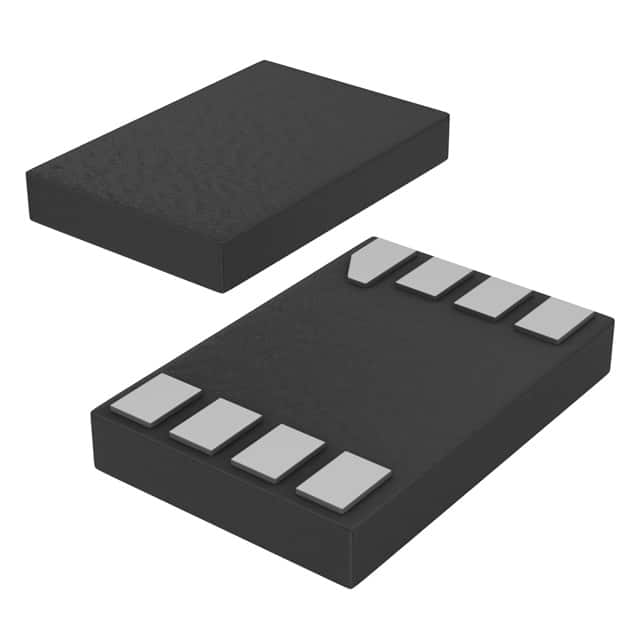
- Package: SOT753 (SC-70-5)
- Essence: This IC is designed to shift logic levels between different voltage domains in digital systems.
- Packaging/Quantity: Available in tape and reel packaging, with a quantity of 3000 units per reel.
Specifications
- Supply Voltage Range: 4.5V to 5.5V
- Input Voltage Range: 0V to VCC
- Output Voltage Range: 0V to VCC
- Maximum Operating Frequency: 400 MHz
- Propagation Delay: 6 ns (typical)
- Output Drive Capability: ±24 mA
- Operating Temperature Range: -40°C to +85°C
Detailed Pin Configuration
The 74AHCT2G125GD,125 IC has a total of 5 pins arranged as follows:
____
   1 |o    | 5
   2 |     | 4
   3 |_____|
Pin 1: Input (A) Pin 2: Output Enable (OE) Pin 3: Ground (GND) Pin 4: Output (Y) Pin 5: Power Supply (VCC)
Functional Features
- Non-Inverting Buffer: The IC provides a non-inverting buffer function, meaning the output signal follows the input signal without any inversion.
- 3-State Output: The output pin can be put into a high-impedance state using the Output Enable (OE) pin, allowing multiple devices to share a common bus without interfering with each other.
- High-Speed Operation: With a maximum operating frequency of 400 MHz, this IC is suitable for high-speed digital systems.
- Low Power Consumption: The 74AHCT2G125GD,125 is designed to operate with low power consumption, making it energy-efficient.
Advantages and Disadvantages
Advantages: - High-speed operation allows for efficient data transfer in digital systems. - Non-inverting buffer preserves the integrity of the input signal. - 3-state output enables bus sharing without interference. - Low power consumption contributes to energy efficiency.
Disadvantages: - Limited voltage range (4.5V to 5.5V) may not be suitable for all applications requiring level shifting. - Propagation delay of 6 ns may introduce timing issues in certain high-frequency applications.
Working Principles
The 74AHCT2G125GD,125 operates based on CMOS technology. It utilizes a combination of MOSFETs (Metal-Oxide-Semiconductor Field-Effect Transistors) to achieve logic level shifting. When an input signal is applied, the IC amplifies and buffers it, providing a non-inverted output signal. The Output Enable (OE) pin controls the state of the output, allowing it to be either active or in a high-impedance state.
Detailed Application Field Plans
The 74AHCT2G125GD,125 is commonly used in various digital systems where logic level shifting is required. Some application fields include: - Microcontrollers and microprocessors - Communication systems - Data acquisition systems - Industrial automation - Consumer electronics
Detailed and Complete Alternative Models
- SN74LVC2G125: Similar logic level shifter with 3-state output, but operates at a wider voltage range (1.65V to 5.5V).
- NC7SZ125: Single-gate logic level shifter with 3-state output, suitable for low-voltage applications (1.65V to 5.5V).
- 74LVC2G07: Dual non-inverting buffer with open-drain output, used for level shifting and signal amplification.
(Note: The above alternative models are provided as examples and may not cover all available options in the market.)
This concludes the encyclopedia entry for the 74AHCT2G125GD,125 IC, covering its basic information, specifications, pin configuration, functional features, advantages and disadvantages, working principles, application field plans, and alternative models.
Liệt kê 10 câu hỏi và câu trả lời thường gặp liên quan đến ứng dụng 74AHCT2G125GD,125 trong giải pháp kỹ thuật
Sure! Here are 10 common questions and answers related to the application of 74AHCT2G125GD,125 in technical solutions:
Q: What is the function of the 74AHCT2G125GD,125? A: The 74AHCT2G125GD,125 is a dual bus buffer gate with 3-state outputs. It is used for signal buffering and level shifting.
Q: What is the operating voltage range of the 74AHCT2G125GD,125? A: The operating voltage range is typically between 4.5V and 5.5V.
Q: Can the 74AHCT2G125GD,125 be used for bidirectional communication? A: Yes, it can be used for bidirectional communication as it has separate input and output pins.
Q: What is the maximum output current of the 74AHCT2G125GD,125? A: The maximum output current is typically around 8mA.
Q: Can the 74AHCT2G125GD,125 handle high-speed signals? A: Yes, it is designed to handle high-speed signals with a propagation delay of typically 6ns.
Q: Is the 74AHCT2G125GD,125 compatible with TTL logic levels? A: Yes, it is compatible with both TTL and CMOS logic levels.
Q: Can I use the 74AHCT2G125GD,125 in automotive applications? A: Yes, it is suitable for automotive applications as it meets the necessary standards and specifications.
Q: Does the 74AHCT2G125GD,125 have built-in ESD protection? A: Yes, it has built-in ESD protection to prevent damage from electrostatic discharge.
Q: Can I use the 74AHCT2G125GD,125 in a battery-powered device? A: Yes, it can be used in battery-powered devices as it operates within a typical voltage range of 4.5V to 5.5V.
Q: Are there any recommended PCB layout guidelines for using the 74AHCT2G125GD,125? A: Yes, it is recommended to follow the manufacturer's guidelines for PCB layout, including proper decoupling and signal routing techniques.
Please note that the answers provided here are general and may vary depending on specific application requirements. It is always recommended to refer to the datasheet and consult with the manufacturer for detailed information.