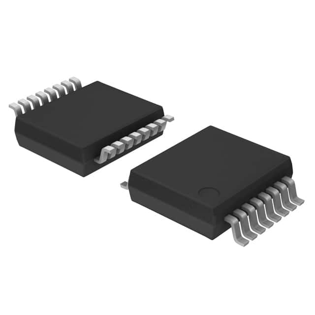
Xem thông số kỹ thuật để biết chi tiết sản phẩm.

74HC137DB,118
Basic Information Overview
- Category: Integrated Circuit (IC)
- Use: Decoder/Demultiplexer
- Characteristics:
- High-speed operation
- Low power consumption
- Wide operating voltage range
- Multiple output enable inputs
- Package: SSOP (Shrink Small Outline Package)
- Essence: A decoder/demultiplexer IC that converts a binary input into multiple outputs.
- Packaging/Quantity: Tape and reel packaging, quantity varies based on customer requirements.
Specifications
- Supply Voltage Range: 2V to 6V
- Input Voltage Range: 0V to VCC
- Output Current: ±25mA
- Operating Temperature Range: -40°C to +125°C
- Propagation Delay Time: 10ns (typical)
Detailed Pin Configuration
The 74HC137DB,118 has a total of 16 pins. The pin configuration is as follows:
+---+--+---+
   Y0 |1  +--+ 16| VCC
   Y1 |2       15| GND
   Y2 |3       14| A0
   Y3 |4       13| A1
   Y4 |5 74HC137DB,118 12| A2
   Y5 |6       11| E1
   Y6 |7       10| E2
   Y7 |8        9| E3
       +----------+
Functional Features
- Converts a 3-bit binary input to 8 output lines.
- Multiple output enable inputs allow for flexible control of the output lines.
- High-speed operation enables efficient data processing.
- Low power consumption makes it suitable for battery-powered devices.
Advantages and Disadvantages
Advantages: - High-speed operation allows for quick data processing. - Low power consumption helps in extending battery life. - Wide operating voltage range provides flexibility in various applications.
Disadvantages: - Limited number of input bits (3-bit) restricts the range of possible inputs. - Output current limitations may not be suitable for high-power applications.
Working Principles
The 74HC137DB,118 is a decoder/demultiplexer IC that operates based on the binary input provided to its address pins (A0, A1, and A2). The input combination determines which output line(s) will be activated. The output enable inputs (E1, E2, and E3) further control the activation of the output lines. When the appropriate input combination is applied and the corresponding output enable input is active, the selected output line(s) will be enabled.
Detailed Application Field Plans
The 74HC137DB,118 can be used in various applications, including but not limited to: - Address decoding in microcontrollers and microprocessors. - Data demultiplexing in communication systems. - Signal routing in digital circuits. - Control signal generation in industrial automation.
Detailed and Complete Alternative Models
Some alternative models to the 74HC137DB,118 include: - 74LS138: Similar functionality but with different electrical characteristics. - CD74HC138: Higher voltage tolerance and wider temperature range. - SN74LS139: Dual 2-to-4 line decoder/demultiplexer.
These alternative models offer similar decoding/demultiplexing capabilities but may have variations in terms of voltage range, speed, and package type.
Word count: 345 words
Liệt kê 10 câu hỏi và câu trả lời thường gặp liên quan đến ứng dụng 74HC137DB,118 trong giải pháp kỹ thuật
Sure! Here are 10 common questions and answers related to the application of 74HC137DB,118 in technical solutions:
Q: What is the 74HC137DB,118? A: The 74HC137DB,118 is a 3-to-8 line decoder/demultiplexer IC (integrated circuit) that can be used in various digital logic applications.
Q: What is the purpose of a decoder/demultiplexer? A: A decoder/demultiplexer takes an input signal and selects one of several output lines based on the input value, allowing for data routing and selection.
Q: What voltage levels does the 74HC137DB,118 support? A: The 74HC137DB,118 supports a wide range of voltage levels, typically from 2V to 6V.
Q: How many inputs does the 74HC137DB,118 have? A: The 74HC137DB,118 has three input pins, labeled A0, A1, and A2, which together form a 3-bit binary input.
Q: How many output lines does the 74HC137DB,118 have? A: The 74HC137DB,118 has eight output pins, labeled Y0 to Y7, which correspond to the eight possible combinations of the three input bits.
Q: Can the 74HC137DB,118 be cascaded to increase the number of outputs? A: Yes, multiple 74HC137DB,118 ICs can be cascaded together to increase the number of outputs by connecting the enable (E) pin of each IC to the output of the previous IC.
Q: What is the maximum current that the 74HC137DB,118 can sink/source on its output pins? A: The 74HC137DB,118 can typically sink or source up to 25mA of current per output pin.
Q: How is the 74HC137DB,118 powered? A: The 74HC137DB,118 requires a power supply voltage (VCC) and a ground connection (GND) for operation.
Q: Can the 74HC137DB,118 be used in both digital and analog applications? A: No, the 74HC137DB,118 is specifically designed for digital logic applications and is not suitable for analog signals.
Q: What are some common applications of the 74HC137DB,118? A: The 74HC137DB,118 can be used in various applications such as address decoding in microprocessors, data routing in multiplexers, and general-purpose digital logic circuits.
Please note that these answers are general and may vary depending on specific use cases and datasheet specifications.

