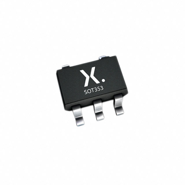
Xem thông số kỹ thuật để biết chi tiết sản phẩm.

74HC1GU04GW,125
Product Overview
Category
The 74HC1GU04GW,125 belongs to the category of integrated circuits (ICs).
Use
This product is commonly used as an inverter, which means it can convert a logic level from high to low or vice versa.
Characteristics
- High-speed operation: The 74HC1GU04GW,125 operates at high speeds, making it suitable for applications that require quick response times.
- Low power consumption: This IC consumes minimal power, making it energy-efficient.
- Wide operating voltage range: It can operate within a wide range of supply voltages, providing flexibility in various applications.
- Small package size: The 74HC1GU04GW,125 comes in a compact package, allowing for space-saving designs.
Package and Quantity
The 74HC1GU04GW,125 is available in a small SOT353 package. It is typically sold in reels containing a specific quantity, such as 3000 units per reel.
Specifications
- Supply voltage range: 2 V to 6 V
- Input voltage range: 0 V to VCC
- Output voltage range: 0 V to VCC
- Maximum input current: ±20 mA
- Maximum output current: ±25 mA
- Operating temperature range: -40°C to +125°C
Pin Configuration
The 74HC1GU04GW,125 has a total of five pins:
- GND (Ground): Connected to the ground reference of the circuit.
- A (Input): Input pin for the logic signal to be inverted.
- Y (Output): Output pin for the inverted logic signal.
- NC (Not Connected): This pin is not connected and should be left unconnected.
- VCC (Supply Voltage): Connected to the positive supply voltage of the circuit.
Functional Features
- Inverting Function: The 74HC1GU04GW,125 performs the function of inverting the logic level applied to its input pin.
- High-Speed Operation: It operates at high speeds, ensuring quick response times in various applications.
- Wide Compatibility: This IC is compatible with a wide range of logic families, making it versatile for integration into different systems.
Advantages and Disadvantages
Advantages
- High-speed operation allows for quick signal processing.
- Low power consumption results in energy-efficient designs.
- Small package size enables space-saving layouts.
- Wide operating voltage range provides flexibility in different applications.
Disadvantages
- Limited functionality: The 74HC1GU04GW,125 only performs the function of an inverter and does not have additional features.
Working Principles
The 74HC1GU04GW,125 utilizes complementary metal-oxide-semiconductor (CMOS) technology to achieve its inverting function. When a logic high voltage is applied to the input pin, the output pin will produce a logic low voltage, and vice versa. This inversion is achieved through the internal circuitry of the IC.
Detailed Application Field Plans
The 74HC1GU04GW,125 can be used in various applications, including but not limited to: - Digital logic circuits - Microcontrollers - Communication systems - Signal processing - Consumer electronics
Alternative Models
There are several alternative models available that offer similar functionality to the 74HC1GU04GW,125. Some popular alternatives include: - SN74LVC1G04DBVR - MC74VHC1G04DTT1G - TC7SZU04FU
These alternative models provide comparable inverting capabilities and can be considered as substitutes based on specific application requirements.
In conclusion, the 74HC1GU04GW,125 is a high-speed, low-power inverter IC that finds applications in various digital systems. Its small package size and wide operating voltage range make it suitable for space-constrained designs. However, it should be noted that this IC has limited functionality and only performs the function of an inverter.
Liệt kê 10 câu hỏi và câu trả lời thường gặp liên quan đến ứng dụng 74HC1GU04GW,125 trong giải pháp kỹ thuật
Sure! Here are 10 common questions and answers related to the application of 74HC1GU04GW,125:
Q1: What is the 74HC1GU04GW,125? A1: The 74HC1GU04GW,125 is a single inverter gate IC (Integrated Circuit) that is commonly used in digital logic circuits.
Q2: What is the voltage supply range for the 74HC1GU04GW,125? A2: The voltage supply range for this IC is typically between 2V and 6V.
Q3: What is the maximum output current of the 74HC1GU04GW,125? A3: The maximum output current is around 4mA.
Q4: Can I use the 74HC1GU04GW,125 in both CMOS and TTL logic circuits? A4: Yes, this IC is compatible with both CMOS and TTL logic levels.
Q5: What is the typical propagation delay of the 74HC1GU04GW,125? A5: The typical propagation delay is around 8ns.
Q6: Can I use the 74HC1GU04GW,125 as a level shifter? A6: Yes, this IC can be used as a level shifter to convert signals between different voltage levels.
Q7: Is the 74HC1GU04GW,125 suitable for high-speed applications? A7: Yes, this IC is designed for high-speed operation and can be used in various high-frequency applications.
Q8: Can I use the 74HC1GU04GW,125 in battery-powered devices? A8: Yes, this IC has a low power consumption and can be used in battery-powered devices.
Q9: Does the 74HC1GU04GW,125 have built-in protection features? A9: No, this IC does not have built-in protection features. External protection components may be required depending on the application.
Q10: Can I use the 74HC1GU04GW,125 in temperature-sensitive environments? A10: Yes, this IC has a wide operating temperature range and can be used in temperature-sensitive environments.
Please note that these answers are general and may vary depending on specific datasheet specifications and application requirements.

