

Xem thông số kỹ thuật để biết chi tiết sản phẩm.
74HCT240BQ-Q100,11
Basic Information Overview
- Category: Integrated Circuit (IC)
- Use: Logic Gate Buffer/Driver
- Characteristics: High-speed, CMOS technology, low power consumption
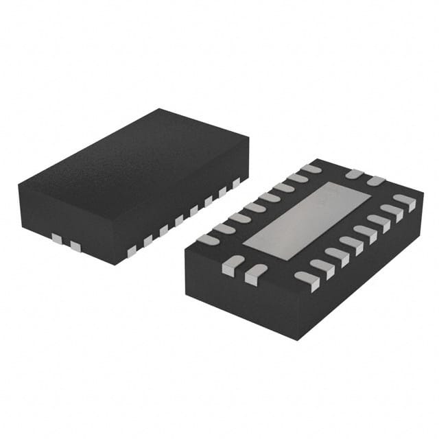
- Package: TSSOP-20
- Essence: Buffer/Driver IC for digital signal amplification and isolation
- Packaging/Quantity: Tape and Reel, 2500 units per reel
Specifications
- Supply Voltage Range: 2.0V to 6.0V
- Input Voltage Range: 0V to VCC
- Output Voltage Range: 0V to VCC
- Operating Temperature Range: -40°C to +125°C
- Propagation Delay: 10 ns (typical)
- Output Current: ±6 mA
Detailed Pin Configuration
- GND (Ground)
- A1 (Input A1)
- B1 (Input B1)
- OE (Output Enable)
- Y1 (Output Y1)
- Y2 (Output Y2)
- B2 (Input B2)
- A2 (Input A2)
- GND (Ground)
- Y3 (Output Y3)
- Y4 (Output Y4)
- B3 (Input B3)
- A3 (Input A3)
- VCC (Supply Voltage)
- B4 (Input B4)
- A4 (Input A4)
- GND (Ground)
- Y5 (Output Y5)
- Y6 (Output Y6)
- B5 (Input B5)
Functional Features
- Buffer/Driver: Amplifies and isolates digital signals
- High-Speed Operation: Suitable for applications requiring fast signal propagation
- CMOS Technology: Low power consumption and wide voltage range compatibility
- Output Enable (OE) Pin: Allows control over the output state
Advantages and Disadvantages
Advantages: - High-speed operation enables efficient signal processing - CMOS technology ensures low power consumption - Wide voltage range compatibility allows versatile applications - Output enable pin provides flexibility in controlling the output state
Disadvantages: - Limited output current may restrict use in certain high-power applications - Propagation delay may affect real-time signal processing in critical systems
Working Principles
The 74HCT240BQ-Q100,11 is a buffer/driver IC that amplifies and isolates digital signals. It operates on CMOS technology, which offers low power consumption and compatibility with a wide voltage range. The IC consists of six buffer gates, each capable of driving one input/output line. The output enable (OE) pin controls the output state, allowing the user to enable or disable the outputs as needed. When the OE pin is high, the outputs are active, and when it is low, the outputs are in a high-impedance state.
Detailed Application Field Plans
The 74HCT240BQ-Q100,11 finds applications in various fields, including: 1. Microcontrollers and Digital Processors: Signal buffering and level shifting between different logic families. 2. Communication Systems: Signal amplification and isolation in data transmission lines. 3. Industrial Automation: Interface between sensors/actuators and control systems. 4. Automotive Electronics: Signal conditioning and level translation in automotive control modules. 5. Consumer Electronics: Signal buffering and level conversion in audio/video equipment.
Detailed and Complete Alternative Models
- SN74HCT240N: DIP-20 package, similar specifications and functionality.
- CD74HCT240E: PDIP-20 package, comparable performance and features.
- MC74HCT240AN: DIP-20 package, equivalent functionality and characteristics.
(Note: The above alternative models are provided for reference and may have slight variations in specifications or packaging.)
This concludes the encyclopedia entry for the 74HCT240BQ-Q100,11.
Liệt kê 10 câu hỏi và câu trả lời thường gặp liên quan đến ứng dụng 74HCT240BQ-Q100,11 trong giải pháp kỹ thuật
Sure! Here are 10 common questions and answers related to the application of 74HCT240BQ-Q100,11 in technical solutions:
Question: What is the function of the 74HCT240BQ-Q100,11?
Answer: The 74HCT240BQ-Q100,11 is an octal buffer/line driver with 3-state outputs. It is used for signal buffering and driving in digital circuits.Question: What is the voltage supply range for this IC?
Answer: The 74HCT240BQ-Q100,11 operates with a voltage supply range of 4.5V to 5.5V.Question: How many input/output pins does it have?
Answer: This IC has 8 input pins and 8 output pins, making it suitable for applications requiring multiple signal lines.Question: Can I use this IC for level shifting between different voltage domains?
Answer: Yes, the 74HCT240BQ-Q100,11 can be used for level shifting as it supports TTL-compatible inputs and CMOS-compatible outputs.Question: What is the maximum output current that this IC can drive?
Answer: The 74HCT240BQ-Q100,11 can drive up to 35mA of current per output pin.Question: Does this IC have built-in protection features?
Answer: Yes, it has built-in protection against electrostatic discharge (ESD) and excessive power dissipation.Question: Can I connect the outputs directly to other ICs or should I use external resistors?
Answer: The outputs of this IC can be connected directly to other ICs without the need for external resistors.Question: Is this IC suitable for high-speed applications?
Answer: Yes, the 74HCT240BQ-Q100,11 is designed for high-speed operation and can handle frequencies up to several megahertz.Question: Can I use this IC in both digital and analog circuits?
Answer: No, this IC is specifically designed for digital applications and may not be suitable for analog circuits.Question: Are there any specific layout considerations when using this IC?
Answer: It is recommended to follow proper PCB layout guidelines, such as minimizing trace lengths and providing adequate decoupling capacitors, to ensure optimal performance of the IC.
Please note that these answers are general and may vary depending on the specific requirements and application context.