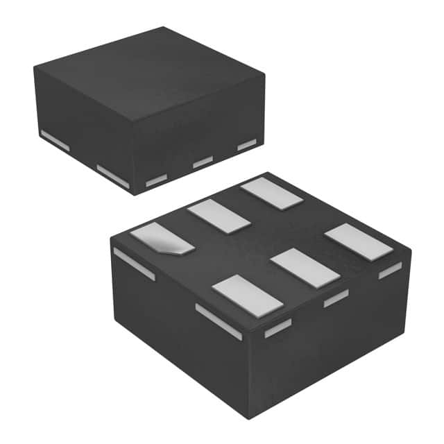
Xem thông số kỹ thuật để biết chi tiết sản phẩm.

74LVC2G07GF,132
Basic Information Overview
- Category: Integrated Circuit (IC)
- Use: Logic Gate Buffer/Driver
- Characteristics:
- Low-voltage CMOS technology
- Dual buffer/driver with open-drain outputs
- High-speed operation
- Wide operating voltage range
- Package: SOT753 (SC-70)
- Essence: This IC is designed to provide buffering and driving capabilities for digital signals in low-voltage applications.
- Packaging/Quantity: Available in tape and reel packaging, with a quantity of 3000 units per reel.
Specifications
- Supply Voltage Range: 1.65V to 5.5V
- Input Voltage Range: 0V to VCC
- Output Voltage Range: 0V to VCC
- Maximum Operating Frequency: 100 MHz
- Propagation Delay: 3.8 ns (typical)
- Output Current: ±24 mA
Detailed Pin Configuration
The 74LVC2G07GF,132 IC has the following pin configuration:
___________
  OE --|           |-- VCC
 I/O1 --|           |-- GND
 I/O2 --|           |-- A
  GND --|           |-- B
       |___________|
Functional Features
- Dual Buffer/Driver: The IC provides two independent buffer/driver circuits.
- Open-Drain Outputs: The outputs are configured as open-drain, allowing them to be connected to other devices or pulled up externally.
- High-Speed Operation: The IC operates at high speeds, making it suitable for time-critical applications.
- Wide Operating Voltage Range: It can operate within a wide voltage range, making it compatible with various systems.
Advantages and Disadvantages
Advantages: - Low-voltage CMOS technology ensures low power consumption. - Small package size allows for space-efficient designs. - Open-drain outputs provide flexibility in interfacing with other devices.
Disadvantages: - Limited output current may not be suitable for driving heavy loads. - Propagation delay may affect timing-sensitive applications.
Working Principles
The 74LVC2G07GF,132 IC operates based on CMOS (Complementary Metal-Oxide-Semiconductor) technology. It uses a combination of NMOS and PMOS transistors to achieve low power consumption and high-speed operation. The inputs are buffered and the outputs are open-drain, allowing for easy integration into various digital systems.
Detailed Application Field Plans
The 74LVC2G07GF,132 IC finds applications in various fields, including but not limited to: 1. Consumer Electronics: Used in smartphones, tablets, and portable devices for signal buffering and driving. 2. Industrial Automation: Employed in control systems and PLCs for signal conditioning and level shifting. 3. Automotive Electronics: Integrated into automotive modules for signal amplification and interfacing. 4. Communication Systems: Utilized in networking equipment and data communication devices for signal processing.
Detailed and Complete Alternative Models
Some alternative models that offer similar functionality to the 74LVC2G07GF,132 IC include: - SN74LVC2G07 from Texas Instruments - MC74VHC2G07 from ON Semiconductor - NCV8402 from ON Semiconductor
These alternatives can be considered based on specific requirements and availability.
Word count: 346 words
Liệt kê 10 câu hỏi và câu trả lời thường gặp liên quan đến ứng dụng 74LVC2G07GF,132 trong giải pháp kỹ thuật
Sure! Here are 10 common questions and answers related to the application of 74LVC2G07GF,132 in technical solutions:
Q: What is the function of the 74LVC2G07GF,132? A: The 74LVC2G07GF,132 is a dual buffer/driver with open-drain outputs. It can be used for level shifting and signal buffering.
Q: What is the operating voltage range of the 74LVC2G07GF,132? A: The 74LVC2G07GF,132 operates within a voltage range of 1.65V to 5.5V.
Q: Can the 74LVC2G07GF,132 handle high-speed signals? A: Yes, the 74LVC2G07GF,132 is designed to handle high-speed signals, making it suitable for applications requiring fast switching.
Q: How many channels does the 74LVC2G07GF,132 have? A: The 74LVC2G07GF,132 has two independent channels, allowing it to buffer or drive two separate signals.
Q: What is the maximum output current of the 74LVC2G07GF,132? A: The 74LVC2G07GF,132 can provide a maximum output current of 24mA per channel.
Q: Can the 74LVC2G07GF,132 be used for bidirectional communication? A: No, the 74LVC2G07GF,132 is not bidirectional. It is primarily used for unidirectional signal buffering or driving.
Q: Is the 74LVC2G07GF,132 compatible with both CMOS and TTL logic levels? A: Yes, the 74LVC2G07GF,132 is compatible with both CMOS and TTL logic levels, making it versatile for various applications.
Q: What is the typical propagation delay of the 74LVC2G07GF,132? A: The typical propagation delay of the 74LVC2G07GF,132 is around 4.5ns.
Q: Can the 74LVC2G07GF,132 be used in automotive applications? A: Yes, the 74LVC2G07GF,132 is AEC-Q100 qualified, making it suitable for automotive applications that require high reliability.
Q: Are there any special considerations when using the 74LVC2G07GF,132 in high-frequency applications? A: In high-frequency applications, it is important to consider the PCB layout and minimize trace lengths to reduce signal degradation and maintain signal integrity.
Please note that these answers are general and may vary depending on specific application requirements. It is always recommended to refer to the datasheet and consult the manufacturer for detailed information.

