

Xem thông số kỹ thuật để biết chi tiết sản phẩm.
74LVC2G125GD,125
Basic Information Overview
- Category: Integrated Circuit (IC)
- Use: Buffer/Driver
- Characteristics: High-speed, low-power, dual bus buffer with 3-state outputs
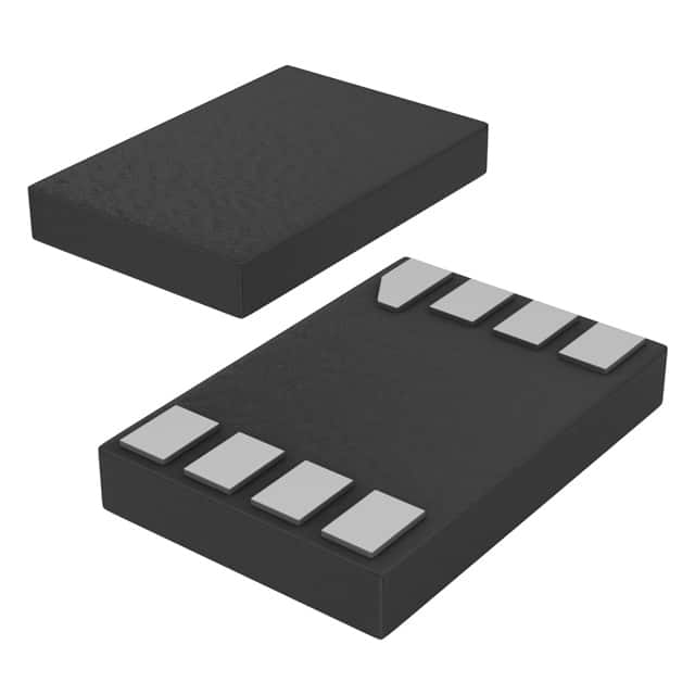
- Package: VSSOP8 (Very Small Outline Plastic Package)
- Essence: This IC is designed to provide buffering and driving capabilities for digital signals in various electronic circuits.
- Packaging/Quantity: Available in reels of 3000 units
Specifications
- Supply Voltage Range: 1.65V to 5.5V
- Input Voltage Range: -0.5V to VCC + 0.5V
- Output Voltage Range: -0.5V to VCC + 0.5V
- Maximum Operating Frequency: 400 MHz
- Output Drive Capability: ±24 mA
- Low Power Consumption: ICC = 2 μA (maximum)
Detailed Pin Configuration
The 74LVC2G125GD,125 IC has a total of 8 pins: 1. Pin 1: Input/Output 1 (IO1) 2. Pin 2: Ground (GND) 3. Pin 3: Input/Output 2 (IO2) 4. Pin 4: Enable Input (OE) 5. Pin 5: Output 2 (Y2) 6. Pin 6: Supply Voltage (VCC) 7. Pin 7: Output 1 (Y1) 8. Pin 8: VCC
Functional Features
- Dual Bus Buffer: Provides independent buffering for two separate input/output signals.
- 3-State Outputs: Allows the outputs to be disabled, effectively disconnecting them from the bus.
- High-Speed Operation: Supports data rates up to 400 MHz, making it suitable for high-speed digital applications.
- Low Power Consumption: Consumes only 2 μA of current when not actively driving the outputs.
- Wide Voltage Range: Can operate with a supply voltage ranging from 1.65V to 5.5V.
Advantages and Disadvantages
Advantages: - High-speed operation enables efficient data transfer in digital circuits. - Low power consumption helps conserve energy in battery-powered devices. - Dual bus buffer allows for independent buffering of two signals. - 3-state outputs provide flexibility in controlling the output state.
Disadvantages: - Limited output drive capability may not be suitable for applications requiring higher current levels. - The VSSOP8 package may be challenging to solder or handle for some users.
Working Principles
The 74LVC2G125GD,125 IC functions as a buffer/driver by amplifying and shaping digital signals. It takes input signals from IO1 and IO2 pins and provides amplified output signals at Y1 and Y2 pins. The OE pin is used to enable or disable the outputs. When the OE pin is low, the outputs are active, and when it is high, the outputs are in a high-impedance state (disconnected).
Detailed Application Field Plans
The 74LVC2G125GD,125 IC finds applications in various electronic systems, including but not limited to: - Communication systems - Computer peripherals - Industrial automation - Consumer electronics - Automotive electronics
Detailed and Complete Alternative Models
Some alternative models that can be considered as alternatives to the 74LVC2G125GD,125 IC are: - SN74LVC2G125DBVR - MC74LCX125DTG - TC7SZ125FU
These alternative models offer similar functionality and characteristics, providing options for designers based on their specific requirements.
Word count: 345 words
Liệt kê 10 câu hỏi và câu trả lời thường gặp liên quan đến ứng dụng 74LVC2G125GD,125 trong giải pháp kỹ thuật
Sure! Here are 10 common questions and answers related to the application of 74LVC2G125GD,125 in technical solutions:
Question: What is the function of the 74LVC2G125GD,125?
Answer: The 74LVC2G125GD,125 is a dual bus buffer gate with 3-state outputs. It can be used for voltage level translation and signal buffering.Question: What is the operating voltage range of the 74LVC2G125GD,125?
Answer: The operating voltage range is from 1.65V to 5.5V.Question: How many inputs and outputs does the 74LVC2G125GD,125 have?
Answer: It has two inputs and two outputs.Question: What is the maximum output current of the 74LVC2G125GD,125?
Answer: The maximum output current is 32mA.Question: Can the 74LVC2G125GD,125 be used for bidirectional level shifting?
Answer: Yes, it can be used for bidirectional level shifting between different voltage domains.Question: What is the propagation delay of the 74LVC2G125GD,125?
Answer: The propagation delay is typically around 4.3ns.Question: Is the 74LVC2G125GD,125 compatible with other logic families?
Answer: Yes, it is compatible with both CMOS and TTL logic families.Question: Can the 74LVC2G125GD,125 drive capacitive loads?
Answer: Yes, it can drive capacitive loads up to 50pF.Question: Does the 74LVC2G125GD,125 have internal pull-up or pull-down resistors?
Answer: No, it does not have internal pull-up or pull-down resistors.Question: What is the package type of the 74LVC2G125GD,125?
Answer: It is available in a small SOT753 package.
Please note that these answers are general and may vary depending on the specific datasheet and manufacturer's specifications for the 74LVC2G125GD,125.