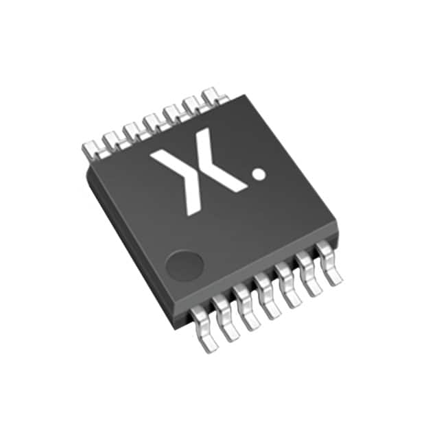
Xem thông số kỹ thuật để biết chi tiết sản phẩm.

74LVT125PW,112
Basic Information Overview
- Category: Integrated Circuit (IC)
- Use: Buffer/Driver
- Characteristics: Low Voltage, Quad Bus Buffer with 3-State Outputs
- Package: TSSOP (Thin Shrink Small Outline Package)
- Essence: This IC is designed to provide buffering and driving capabilities for digital signals in low voltage applications.
- Packaging/Quantity: Available in tape and reel packaging, with a quantity of 2500 units per reel.
Specifications
- Supply Voltage Range: 1.65V to 3.6V
- Input Voltage Range: -0.5V to VCC + 0.5V
- Output Voltage Range: 0V to VCC
- Operating Temperature Range: -40°C to +85°C
- Output Drive Capability: ±24mA at 3.0V
- Propagation Delay Time: 2.8ns (typical) at 3.3V
- Maximum Quiescent Current: 10μA at 3.3V
Detailed Pin Configuration
The 74LVT125PW,112 IC has a total of 14 pins, which are assigned as follows:
Pin | Name | Description --- | ---- | ----------- 1 | OE | Output Enable Input 2 | Y1 | Output 1 3 | GND | Ground 4 | Y2 | Output 2 5 | Y3 | Output 3 6 | VCC | Power Supply 7 | A1 | Input 1 8 | A2 | Input 2 9 | A3 | Input 3 10 | A4 | Input 4 11 | GND | Ground 12 | Y4 | Output 4 13 | OE | Output Enable Input 14 | VCC | Power Supply
Functional Features
- Quad bus buffer with 3-state outputs.
- Inputs and outputs are tolerant to 5.5V, allowing for direct interface with TTL/CMOS devices.
- Provides non-inverting buffer functions.
- Outputs can be disabled using the output enable (OE) input, which puts them in a high-impedance state.
Advantages and Disadvantages
Advantages: - Low voltage operation makes it suitable for battery-powered applications. - High-speed operation allows for efficient signal buffering. - 3-state outputs provide flexibility in controlling signal flow.
Disadvantages: - Limited output drive capability compared to some other buffer ICs. - Not suitable for high-voltage applications.
Working Principles
The 74LVT125PW,112 operates by receiving digital signals at its input pins (A1-A4) and buffering them to the corresponding output pins (Y1-Y4). The output enable (OE) input controls whether the outputs are active or in a high-impedance state. When OE is low, the outputs are enabled and mirror the input signals. When OE is high, the outputs are disabled and enter a high-impedance state.
Detailed Application Field Plans
The 74LVT125PW,112 is commonly used in various applications, including: - Microprocessor systems - Data communication systems - Networking equipment - Industrial automation - Consumer electronics
Detailed and Complete Alternative Models
Some alternative models that offer similar functionality to the 74LVT125PW,112 include: - SN74LVC125A: Low Voltage Quad Buffer/Driver with 3-State Outputs - MC74LVX125: Low Voltage CMOS Quad Buffer with 3-State Outputs - 74HC125: Quad Bus Buffer with 3-State Outputs
These alternative models can be considered based on specific requirements and availability.
Word count: 346 words
Liệt kê 10 câu hỏi và câu trả lời thường gặp liên quan đến ứng dụng 74LVT125PW,112 trong giải pháp kỹ thuật
Sure! Here are 10 common questions and answers related to the application of 74LVT125PW,112 in technical solutions:
Q: What is the function of the 74LVT125PW,112? A: The 74LVT125PW,112 is a quad buffer/line driver with 3-state outputs.
Q: What is the operating voltage range for the 74LVT125PW,112? A: The operating voltage range is typically between 1.65V and 3.6V.
Q: Can the 74LVT125PW,112 be used in both digital and analog applications? A: No, it is primarily designed for digital applications.
Q: What is the maximum output current that the 74LVT125PW,112 can handle? A: The maximum output current is typically around ±24mA.
Q: Is the 74LVT125PW,112 compatible with TTL logic levels? A: Yes, it is compatible with both TTL and CMOS logic levels.
Q: Can the 74LVT125PW,112 be used as a level shifter? A: Yes, it can be used as a level shifter to convert signals between different voltage levels.
Q: Does the 74LVT125PW,112 have built-in protection against electrostatic discharge (ESD)? A: Yes, it has ESD protection on all inputs and outputs.
Q: What is the typical propagation delay of the 74LVT125PW,112? A: The typical propagation delay is around 3.5ns.
Q: Can the 74LVT125PW,112 drive capacitive loads? A: Yes, it can drive capacitive loads up to a certain limit specified in the datasheet.
Q: Is the 74LVT125PW,112 available in different package options? A: Yes, it is available in various package options such as TSSOP, SOIC, and SSOP.
Please note that the answers provided here are general and may vary depending on the specific datasheet and manufacturer's specifications for the 74LVT125PW,112.

