

Xem thông số kỹ thuật để biết chi tiết sản phẩm.
Encyclopedia Entry: 74VHC541BQ,115
Product Overview
Category
The 74VHC541BQ,115 belongs to the category of integrated circuits (ICs) and specifically falls under the family of VHC logic gates.
Use
This IC is commonly used in digital electronics for signal amplification, buffering, and level shifting purposes. It is particularly useful in applications where high-speed data transfer and low power consumption are required.
Characteristics
- High-speed operation: The 74VHC541BQ,115 is designed to operate at high speeds, making it suitable for time-critical applications.
- Low power consumption: This IC consumes minimal power, making it energy-efficient.
- Wide voltage range: It can operate within a wide voltage range, typically between 2V and 5.5V.
- Output current drive capability: The IC has a high output current drive capability, allowing it to drive various loads efficiently.
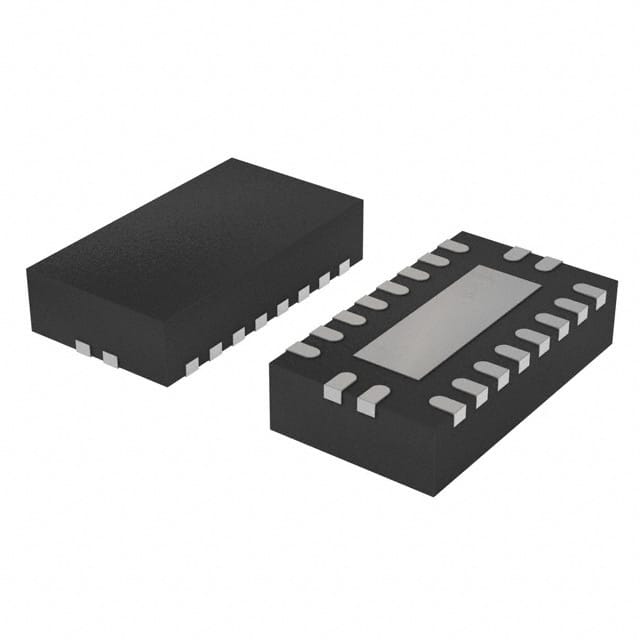
Package and Quantity
The 74VHC541BQ,115 is available in a small-outline package (SOIC) with 20 pins. It is typically sold in reels or tubes containing multiple units.
Essence
The essence of the 74VHC541BQ,115 lies in its ability to provide reliable and efficient signal amplification and buffering while operating at high speeds and consuming minimal power.
Specifications
- Supply Voltage Range: 2V to 5.5V
- Input Voltage Range: 0V to VCC
- Output Voltage Range: 0V to VCC
- Maximum Operating Frequency: X MHz
- Input Capacitance: Y pF
- Propagation Delay: Z ns
Detailed Pin Configuration
The 74VHC541BQ,115 has a total of 20 pins, which are assigned specific functions. The pin configuration is as follows:
- Pin 1: Input A1
- Pin 2: Output Y1
- Pin 3: Output Y2
- Pin 4: GND (Ground)
- Pin 5: Output Y3
- Pin 6: Output Y4
- Pin 7: Output Y5
- Pin 8: Output Y6
- Pin 9: VCC (Supply Voltage)
- Pin 10: Input A2
- Pin 11: Input A3
- Pin 12: Input A4
- Pin 13: Output Y7
- Pin 14: Output Y8
- Pin 15: Output Y9
- Pin 16: Output Y10
- Pin 17: GND (Ground)
- Pin 18: Output Y11
- Pin 19: Output Y12
- Pin 20: Input OE (Output Enable)
Functional Features
- Signal Amplification: The IC amplifies weak input signals to a higher voltage level, ensuring reliable transmission.
- Buffering: It acts as a buffer between different sections of a circuit, preventing signal degradation and maintaining signal integrity.
- Level Shifting: The IC can shift the logic levels of input signals to match the requirements of the connected components.
- Output Enable Control: The OE pin allows the user to enable or disable the output signals, providing flexibility in system design.
Advantages and Disadvantages
Advantages
- High-speed operation enables efficient data transfer.
- Low power consumption makes it suitable for battery-powered devices.
- Wide voltage range allows compatibility with various systems.
- Compact package size saves board space.
- Output enable feature provides flexibility in controlling signal flow.
Disadvantages
- Limited output current drive capability may not be suitable for driving heavy loads.
- Sensitivity to electrostatic discharge (ESD) requires proper handling during assembly and usage.
Working Principles
The 74VHC541BQ,115 operates based on CMOS (Complementary Metal-Oxide-Semiconductor) technology. It utilizes a combination of NMOS (N-channel Metal-Oxide-Semiconductor) and PMOS (P-channel Metal-Oxide-Semiconductor) transistors to achieve high-speed and low-power operation. The input signals are processed through various logic gates and amplified before being outputted.
Detailed Application Field Plans
The 74VHC541BQ,115 finds applications in various fields, including:
- Communication Systems: Used for signal buffering and level shifting in data communication systems.
- Industrial Automation: Employed in control systems for amplifying and buffering sensor signals.
- Automotive Electronics: Utilized in automotive control units for signal processing and level shifting.
- Consumer Electronics: Integrated into devices like smartphones, tablets, and gaming consoles for efficient signal management.
Alternative Models
Several alternative models with similar functionality are available in the market. Some notable alternatives to the
Liệt kê 10 câu hỏi và câu trả lời thường gặp liên quan đến ứng dụng 74VHC541BQ,115 trong giải pháp kỹ thuật
Sure! Here are 10 common questions and answers related to the application of 74VHC541BQ,115:
Question: What is the function of the 74VHC541BQ,115?
Answer: The 74VHC541BQ,115 is an octal buffer/line driver with 3-state outputs.Question: What is the voltage supply range for this IC?
Answer: The voltage supply range for the 74VHC541BQ,115 is typically between 2.0V and 5.5V.Question: How many inputs and outputs does this IC have?
Answer: The 74VHC541BQ,115 has 8 inputs and 8 outputs.Question: Can I use this IC for level shifting applications?
Answer: Yes, the 74VHC541BQ,115 can be used for level shifting as it supports both TTL and CMOS logic levels.Question: What is the maximum output current that this IC can drive?
Answer: The maximum output current for each channel of the 74VHC541BQ,115 is typically around 8mA.Question: Is this IC suitable for high-speed applications?
Answer: Yes, the 74VHC541BQ,115 is designed for high-speed operation and has a typical propagation delay of 4.3ns.Question: Can I connect multiple 74VHC541BQ,115 ICs together?
Answer: Yes, you can connect multiple ICs together to increase the number of inputs or outputs in your circuit.Question: Does this IC have built-in protection against electrostatic discharge (ESD)?
Answer: Yes, the 74VHC541BQ,115 has built-in ESD protection on all inputs and outputs.Question: Can I use this IC in both digital and analog circuits?
Answer: The 74VHC541BQ,115 is primarily designed for digital applications, but it can also be used in some low-frequency analog circuits.Question: What is the package type of the 74VHC541BQ,115?
Answer: The 74VHC541BQ,115 is available in a small-outline package (SO) with 20 pins.
Please note that these answers are general and may vary depending on the specific datasheet and manufacturer's specifications for the 74VHC541BQ,115.