

Xem thông số kỹ thuật để biết chi tiết sản phẩm.
PDTC114YT,215
Product Overview
- Belongs to: Semiconductor category
- Use: Signal switching and amplification in electronic circuits
- Characteristics: Small form factor, high gain, low power consumption
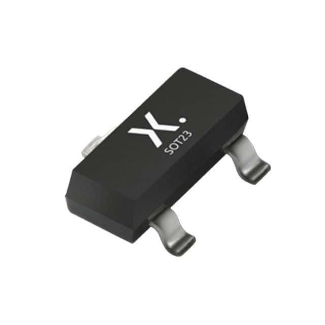
- Package: SOT416 (SC-75)
- Essence: NPN bipolar junction transistor
- Packaging/Quantity: Tape and reel, 3000 units per reel
Specifications
- Collector-Base Voltage (VCBO): 50V
- Collector-Emitter Voltage (VCEO): 45V
- Emitter-Base Voltage (VEBO): 5V
- Collector Current (IC): 100mA
- Power Dissipation (Ptot): 200mW
- Transition Frequency (fT): 250MHz
- Noise Figure (NF): 4dB
Detailed Pin Configuration
- Collector (C)
- Base (B)
- Emitter (E)
Functional Features
- High current gain
- Low noise figure
- Fast switching speed
Advantages
- Small package size
- Suitable for high-frequency applications
- Low power consumption
Disadvantages
- Limited collector current capability
- Susceptible to thermal runaway at high currents
Working Principles
The PDTC114YT,215 operates as a signal amplifier or switch by controlling the flow of current between its collector and emitter terminals based on the input signal applied to its base terminal.
Detailed Application Field Plans
- Audio amplification circuits
- Radio frequency (RF) signal amplification
- Switching circuits in communication systems
Detailed and Complete Alternative Models
- BC847B,235
- MMBT3904LT1G
- 2N3904
This comprehensive entry provides an in-depth understanding of the PDTC114YT,215 semiconductor, covering its specifications, features, advantages, disadvantages, working principles, application field plans, and alternative models.
Liệt kê 10 câu hỏi và câu trả lời thường gặp liên quan đến ứng dụng PDTC114YT,215 trong giải pháp kỹ thuật
What is the PDTC114YT,215 used for?
- The PDTC114YT,215 is commonly used as a general-purpose NPN transistor in various technical solutions.
What are the key specifications of the PDTC114YT,215?
- The PDTC114YT,215 has a maximum collector current of 100mA, a maximum collector-emitter voltage of 50V, and a DC current gain (hFE) of 100 to 400.
Can the PDTC114YT,215 be used for switching applications?
- Yes, the PDTC114YT,215 can be used for low-power switching applications due to its moderate current and voltage ratings.
Is the PDTC114YT,215 suitable for amplification purposes?
- The PDTC114YT,215 can be used for small-signal amplification in low-power circuits.
What are the typical operating conditions for the PDTC114YT,215?
- The PDTC114YT,215 operates within a temperature range of -55°C to 150°C and is suitable for use in various electronic devices.
Does the PDTC114YT,215 require any specific biasing or drive circuitry?
- The PDTC114YT,215 requires standard NPN transistor biasing and drive circuitry for proper operation.
Are there any common alternative transistors to the PDTC114YT,215?
- Some common alternatives to the PDTC114YT,215 include the 2N3904, BC547, and PN2222A transistors, which have similar characteristics.
What are the typical applications of the PDTC114YT,215 in technical solutions?
- The PDTC114YT,215 is often used in low-power amplifiers, signal processing circuits, and general switching applications.
What are the recommended soldering and handling practices for the PDTC114YT,215?
- It is recommended to follow standard ESD (electrostatic discharge) precautions and soldering guidelines when handling the PDTC114YT,215 to prevent damage.
Where can I find detailed technical documentation for the PDTC114YT,215?
- Detailed technical documentation for the PDTC114YT,215 can be found in the datasheet provided by the manufacturer, which includes electrical characteristics, package information, and application notes.