

Xem thông số kỹ thuật để biết chi tiết sản phẩm.
Encyclopedia Entry: 74ALVCHS16830DGB,1
Product Overview
Category
The 74ALVCHS16830DGB,1 belongs to the category of integrated circuits (ICs) and specifically falls under the family of digital logic devices.
Use
This product is commonly used in electronic systems for data processing and manipulation. It serves as a buffer/line driver with 18-bit universal bus transceiver functionality.
Characteristics
- High-speed operation
- Low power consumption
- Wide voltage range compatibility
- Robust ESD performance
- Compact package size
Package
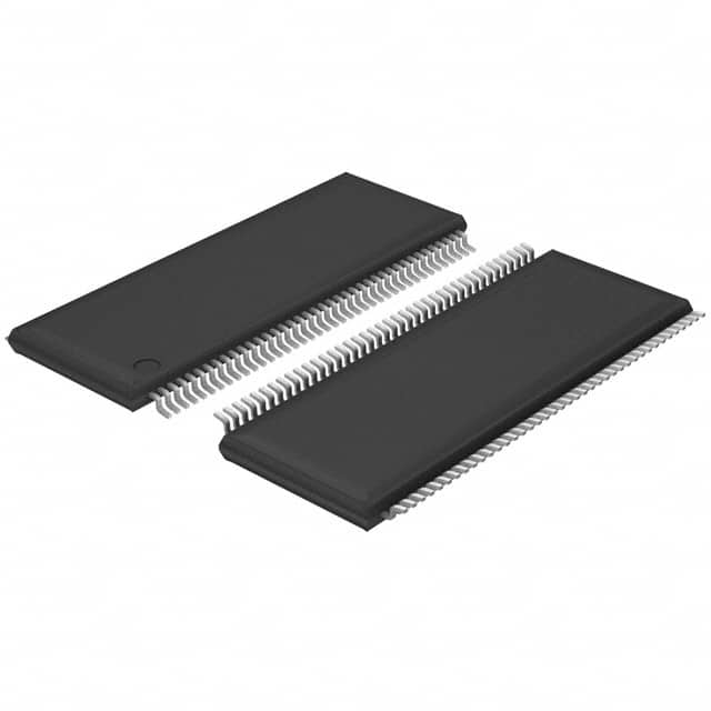
The 74ALVCHS16830DGB,1 is available in a small form factor package, such as a 56-pin TSSOP (Thin Shrink Small Outline Package).
Essence
The essence of this product lies in its ability to provide bidirectional buffering and voltage level translation for digital signals in various electronic applications.
Packaging/Quantity
Typically, the 74ALVCHS16830DGB,1 is supplied in reels or tubes, containing a quantity of 250 units per package.
Specifications
- Supply Voltage Range: 1.2V to 3.6V
- Input Voltage Range: -0.5V to VCC + 0.5V
- Output Voltage Range: 0V to VCC
- Operating Temperature Range: -40°C to +85°C
- Propagation Delay Time: 2.5ns (max)
- Output Current: ±24mA
Detailed Pin Configuration
The pin configuration of the 74ALVCHS16830DGB,1 is as follows:
+-------------------+
   OE1 |1                 56| VCC
   A1  |2                 55| B1
   Y1  |3                 54| A2
   B2  |4                 53| Y2
   A3  |5                 52| B3
   Y3  |6                 51| A4
   B4  |7                 50| Y4
   A5  |8                 49| B5
   Y5  |9                 48| A6
   B6  |10                47| Y6
   A7  |11                46| B7
   Y7  |12                45| A8
   B8  |13                44| Y8
   A9  |14                43| B9
   Y9  |15                42| A10
   B10 |16                41| Y10
   A11 |17                40| B11
   Y11 |18                39| A12
   B12 |19                38| Y12
   A13 |20                37| B13
   Y13 |21                36| A14
   B14 |22                35| Y14
   A15 |23                34| B15
   Y15 |24                33| A16
   B16 |25                32| Y16
   GND |26                31| B17
   OE2 |27                30| Y17
   A17 |28                29| B18
       +-------------------+
Functional Features
- Bidirectional data transmission
- Voltage level translation
- Output enable control for bus sharing
- High-speed operation for efficient data transfer
- Low power consumption for energy efficiency
- Robust electrostatic discharge (ESD) protection
Advantages and Disadvantages
Advantages
- High-speed operation enables fast data processing.
- Wide voltage range compatibility allows for versatile integration in various systems.
- Low power consumption contributes to energy-efficient designs.
- Robust ESD performance ensures reliable operation in challenging environments.
Disadvantages
- Limited number of input/output pins (18-bit) may restrict the complexity of certain applications.
- The small package size may require additional care during handling and soldering.
Working Principles
The 74ALVCHS16830DGB,1 operates by receiving digital signals on its input pins and providing corresponding output signals on the output pins. It incorporates internal circuitry that facilitates bidirectional data transmission and voltage level translation. The output enable control pin allows for bus sharing among multiple devices. The device operates within a specified voltage range and provides high-speed data transfer with minimal propagation delay.
Detailed Application Field Plans
The 74ALVCHS16830DGB,1 finds application in various electronic systems, including but not limited to: - Microprocessors and microcontrollers - Data communication systems - Memory interfaces - Industrial automation equipment - Consumer electronics
Liệt kê 10 câu hỏi và câu trả lời thường gặp liên quan đến ứng dụng 74ALVCHS16830DGB,1 trong giải pháp kỹ thuật
Sure! Here are 10 common questions and answers related to the application of 74ALVCHS16830DGB,1 in technical solutions:
Q1: What is the function of the 74ALVCHS16830DGB,1? A1: The 74ALVCHS16830DGB,1 is a 18-bit universal bus driver with 3-state outputs. It can be used to drive data buses in various digital systems.
Q2: What is the operating voltage range for this device? A2: The 74ALVCHS16830DGB,1 operates within a voltage range of 1.65V to 3.6V.
Q3: How many output pins does it have? A3: The 74ALVCHS16830DGB,1 has 18 output pins, corresponding to the 18 bits of the bus it drives.
Q4: Can this device handle high-speed data transmission? A4: Yes, the 74ALVCHS16830DGB,1 is designed for high-speed operation and can support data rates up to several hundred megahertz.
Q5: Is this device compatible with other logic families? A5: Yes, the 74ALVCHS16830DGB,1 is designed to be compatible with both TTL and CMOS logic families.
Q6: Does this device have built-in protection features? A6: Yes, the 74ALVCHS16830DGB,1 includes ESD protection on all inputs and outputs, providing robustness against electrostatic discharge events.
Q7: Can I use this device in a bidirectional bus configuration? A7: No, the 74ALVCHS16830DGB,1 is a unidirectional bus driver and does not support bidirectional bus configurations.
Q8: What is the maximum output current this device can provide? A8: The 74ALVCHS16830DGB,1 can source or sink up to 24mA of current per output pin.
Q9: Can I use this device in a hot-swappable application? A9: Yes, the 74ALVCHS16830DGB,1 supports hot insertion and removal of the device without causing damage to the circuit.
Q10: Are there any specific layout considerations for using this device? A10: Yes, it is recommended to follow the manufacturer's guidelines for proper PCB layout, including minimizing trace lengths and providing adequate decoupling capacitors near the device.
Please note that these answers are general and may vary depending on the specific requirements and datasheet of the 74ALVCHS16830DGB,1.