

Xem thông số kỹ thuật để biết chi tiết sản phẩm.
MC13892DJVLR2
Product Overview
- Category: Integrated Circuit (IC)
- Use: Power Management IC
- Characteristics: High-performance, low-power consumption
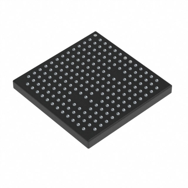
- Package: Small outline package (SOP), 48 pins
- Essence: Efficient power management for electronic devices
- Packaging/Quantity: Tape and reel packaging, quantity varies based on customer requirements
Specifications
- Input Voltage Range: 2.7V to 5.5V
- Output Voltage Range: 0.8V to 3.6V
- Operating Temperature Range: -40°C to +85°C
- Maximum Current Output: 1A
- Standby Current: <1µA
- Switching Frequency: 2MHz
Detailed Pin Configuration
The MC13892DJVLR2 has a total of 48 pins. Here is a detailed pin configuration:
- VBAT
- VDDRF
- VDDPA
- VDDTX
- VDDRX
- VDDHS
- VDDPLL
- VDDMX
- VDDIO_1P8
- VDDIO_2P8
- VDDIO_3P0
- VDDIO_3P3
- VDDIO_3P6
- VDDIO_3P8
- VDDIO_4P0
- VDDIO_4P2
- VDDIO_4P4
- VDDIO_4P6
- VDDIO_4P8
- VDDIO_5P0
- VDDIO_5P2
- VDDIO_5P4
- VDDIO_5P6
- VDDIO_5P8
- VDDIO_6P0
- VDDIO_6P2
- VDDIO_6P4
- VDDIO_6P6
- VDDIO_6P8
- VDDIO_7P0
- VDDIO_7P2
- VDDIO_7P4
- VDDIO_7P6
- VDDIO_7P8
- VDDIO_8P0
- VDDIO_8P2
- VDDIO_8P4
- VDDIO_8P6
- VDDIO_8P8
- VDDIO_9P0
- VDDIO_9P2
- VDDIO_9P4
- VDDIO_9P6
- VDDIO_9P8
- VDDIO_10P0
- VDDIO_10P2
- VDDIO_10P4
- VDDIO_10P6
Functional Features
- Power management for various electronic devices
- Efficient voltage regulation and current control
- Overcurrent protection
- Thermal shutdown protection
- Low standby power consumption
- Wide input voltage range
- High switching frequency for improved efficiency
Advantages and Disadvantages
Advantages
- High-performance power management solution
- Low-power consumption for extended battery life
- Compact package size for space-constrained applications
- Wide input voltage range allows compatibility with different power sources
- Comprehensive pin configuration for versatile usage
Disadvantages
- Limited maximum current output of 1A
- Operating temperature range may not be suitable for extreme environments
Working Principles
The MC13892DJVLR2 is designed to efficiently manage power in electronic devices. It regulates input voltage, controls output voltage levels, and provides overcurrent and thermal protection. The integrated circuit utilizes switching techniques to achieve high efficiency and low power consumption.
Detailed Application Field Plans
The MC13892DJVLR2 finds applications in various electronic devices, including but not limited to:
- Smartphones
- Tablets
- Portable gaming consoles
- Wearable devices
- IoT (Internet of Things) devices
- Medical devices
- Industrial equipment
- Automotive electronics
Detailed and Complete Alternative Models
- MC13892DJVL: Similar specifications and features, different pin configuration
- MC13892DJVLR: Same pin configuration, extended temperature range
- MC13892DJVLT: Same pin configuration, lower standby current
- MC13892DJVLS: Same pin configuration, optimized for space-constrained applications
Note: The above alternative models are provided as examples and may vary based on specific requirements and
Liệt kê 10 câu hỏi và câu trả lời thường gặp liên quan đến ứng dụng MC13892DJVLR2 trong giải pháp kỹ thuật
Sure! Here are 10 common questions and answers related to the application of MC13892DJVLR2 in technical solutions:
Q: What is MC13892DJVLR2? A: MC13892DJVLR2 is a power management integrated circuit (PMIC) designed for use in various technical solutions.
Q: What are the key features of MC13892DJVLR2? A: Some key features of MC13892DJVLR2 include multiple voltage regulators, battery charging capabilities, power sequencing, and various protection mechanisms.
Q: What technical solutions can MC13892DJVLR2 be used in? A: MC13892DJVLR2 can be used in a wide range of applications such as smartphones, tablets, portable media players, and other battery-powered devices.
Q: How does MC13892DJVLR2 help in power management? A: MC13892DJVLR2 provides efficient power conversion, voltage regulation, and power sequencing, ensuring optimal power delivery to different components of a system.
Q: Can MC13892DJVLR2 handle battery charging? A: Yes, MC13892DJVLR2 has built-in battery charging capabilities, supporting various battery chemistries and charging profiles.
Q: Does MC13892DJVLR2 offer any protection features? A: Yes, MC13892DJVLR2 includes protection mechanisms like overvoltage protection, undervoltage lockout, thermal shutdown, and short-circuit protection.
Q: Is MC13892DJVLR2 programmable? A: Yes, MC13892DJVLR2 is programmable through an I2C interface, allowing customization of various parameters and settings.
Q: What is the input voltage range supported by MC13892DJVLR2? A: MC13892DJVLR2 supports an input voltage range of typically 3.6V to 5.5V.
Q: Can MC13892DJVLR2 operate in low-power modes? A: Yes, MC13892DJVLR2 offers different low-power modes to optimize power consumption during standby or idle periods.
Q: Are there any evaluation boards or reference designs available for MC13892DJVLR2? A: Yes, NXP provides evaluation boards and reference designs that can help developers quickly prototype and integrate MC13892DJVLR2 into their solutions.
Please note that these answers are general and may vary depending on specific implementation requirements and datasheet specifications.