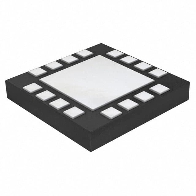
Xem thông số kỹ thuật để biết chi tiết sản phẩm.

NX3DV3899HR,115
Product Overview
- Category: Integrated Circuit (IC)
- Use: Digital Multiplexer/Demultiplexer
- Characteristics:
- High-speed switching capability
- Low power consumption
- Small package size
- Wide operating voltage range
- Package: HR (Housed in a small plastic package with exposed pad for heat dissipation)
- Essence: This IC is designed to provide digital multiplexing and demultiplexing functionality in various electronic systems.
- Packaging/Quantity: Available in tape and reel packaging, with 3000 units per reel.
Specifications
- Supply Voltage Range: 1.65V to 5.5V
- Operating Temperature Range: -40°C to +85°C
- Input Signal Voltage Range: GND to VDD
- Maximum On-State Resistance: 4Ω
- Maximum On-State Current: ±250mA
- Maximum Off-State Leakage Current: ±10nA
- Maximum Propagation Delay Time: 2.5ns
Detailed Pin Configuration
The NX3DV3899HR,115 IC has a total of 16 pins, which are assigned as follows:
- IN0: Input 0
- IN1: Input 1
- IN2: Input 2
- IN3: Input 3
- EN: Enable Input
- S0: Select Input 0
- S1: Select Input 1
- S2: Select Input 2
- Y0: Output 0
- Y1: Output 1
- Y2: Output 2
- Y3: Output 3
- GND: Ground
- NC: No Connection
- VDD: Power Supply
- PAD: Exposed Pad for Heat Dissipation
Functional Features
- Digital multiplexing and demultiplexing of four input signals
- High-speed switching capability allows for efficient data transmission
- Low power consumption ensures energy efficiency
- Wide operating voltage range provides compatibility with various systems
- Enable input allows for control over the output state
- Small package size saves board space in electronic designs
Advantages and Disadvantages
Advantages: - High-speed switching capability enables fast data transmission - Low power consumption contributes to energy efficiency - Wide operating voltage range enhances compatibility - Small package size saves board space
Disadvantages: - Limited number of input and output channels (4:1 multiplexer/demultiplexer) - May not be suitable for applications requiring a higher number of channels
Working Principles
The NX3DV3899HR,115 IC operates based on the principles of digital multiplexing and demultiplexing. It uses internal circuitry to select and route one of the four input signals to the output based on the control inputs. The enable input allows for enabling or disabling the output. When enabled, the selected input signal is transmitted to the corresponding output.
Detailed Application Field Plans
The NX3DV3899HR,115 IC finds applications in various electronic systems, including but not limited to:
- Data communication systems
- Telecommunication equipment
- Audio/video signal routing
- Test and measurement instruments
- Industrial automation systems
Detailed and Complete Alternative Models
- CD74HC4051E: 8-channel analog multiplexer/demultiplexer
- SN74LVC1G3157DBVR: Single-channel analog switch/multiplexer
- ADG732BSUZ: 32-channel analog multiplexer/demultiplexer
- MAX4617CSE+: Quad SPST analog switch
- TS3A5017DGVR: Single-channel bidirectional analog switch
These alternative models offer different channel configurations and features, providing options for various application requirements.
Word count: 400 words
Liệt kê 10 câu hỏi và câu trả lời thường gặp liên quan đến ứng dụng NX3DV3899HR,115 trong giải pháp kỹ thuật
Sure! Here are 10 common questions and answers related to the application of NX3DV3899HR,115 in technical solutions:
Q: What is the NX3DV3899HR,115? A: The NX3DV3899HR,115 is a high-speed, low-power, dual-supply voltage level translator IC.
Q: What are the key features of the NX3DV3899HR,115? A: The key features include bidirectional voltage translation, support for multiple voltage levels, low power consumption, and high-speed operation.
Q: What is the typical application of the NX3DV3899HR,115? A: The NX3DV3899HR,115 is commonly used in applications where voltage translation is required between different logic levels, such as in mixed-voltage systems or interfacing between microcontrollers and peripherals.
Q: What voltage levels does the NX3DV3899HR,115 support? A: The NX3DV3899HR,115 supports voltage translation between two supply voltages ranging from 1.2V to 3.6V.
Q: How many channels does the NX3DV3899HR,115 have? A: The NX3DV3899HR,115 has two independent bidirectional channels, allowing simultaneous translation of signals in both directions.
Q: What is the maximum data rate supported by the NX3DV3899HR,115? A: The NX3DV3899HR,115 can support data rates up to 100 Mbps.
Q: Does the NX3DV3899HR,115 require external components for operation? A: Yes, the NX3DV3899HR,115 requires external pull-up resistors and decoupling capacitors for proper operation.
Q: Can the NX3DV3899HR,115 handle level shifting between different voltage domains? A: Yes, the NX3DV3899HR,115 is designed to handle level shifting between different voltage domains, ensuring reliable communication between devices operating at different logic levels.
Q: Is the NX3DV3899HR,115 compatible with both CMOS and TTL logic levels? A: Yes, the NX3DV3899HR,115 is compatible with both CMOS and TTL logic levels, making it versatile for various applications.
Q: What is the package type of the NX3DV3899HR,115? A: The NX3DV3899HR,115 is available in a compact 16-pin TSSOP package, which is suitable for space-constrained designs.
Please note that these answers are general and may vary depending on specific application requirements.

