

Xem thông số kỹ thuật để biết chi tiết sản phẩm.
NX3L1G3157GW,125
Basic Information Overview
- Category: Integrated Circuit (IC)
- Use: Analog Switch
- Characteristics:
- Low voltage operation
- High bandwidth
- Low ON-resistance
- Wide supply voltage range
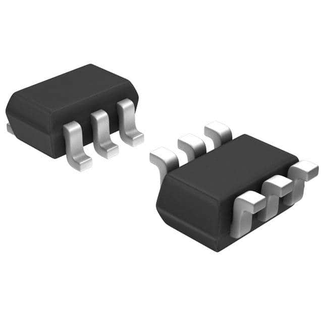
- Package: SOT753
- Essence: Analog switch for signal routing applications
- Packaging/Quantity: Tape and Reel, 3000 pieces per reel
Specifications
- Supply Voltage Range: 1.65V to 5.5V
- ON-Resistance: 0.4Ω (typical) at VCC = 4.5V
- Bandwidth: 400MHz (typical) at VCC = 4.5V
- Leakage Current: 1nA (typical) at VCC = 5.5V
- Operating Temperature Range: -40°C to +85°C
Detailed Pin Configuration
The NX3L1G3157GW,125 has a total of six pins: 1. Pin 1: IN (Input) 2. Pin 2: GND (Ground) 3. Pin 3: COM (Common) 4. Pin 4: NO (Normally Open) 5. Pin 5: NC (Normally Closed) 6. Pin 6: VCC (Supply Voltage)
Functional Features
- Single-pole single-throw (SPST) analog switch
- Bidirectional signal routing capability
- Break-before-make switching action
- Low power consumption
- ESD protection up to 2kV (HBM)
Advantages and Disadvantages
Advantages: - Wide supply voltage range allows compatibility with various systems - Low ON-resistance minimizes signal distortion - High bandwidth enables transmission of high-frequency signals - Small package size saves board space
Disadvantages: - Limited number of channels (single channel) - Not suitable for high-power applications
Working Principles
The NX3L1G3157GW,125 is an analog switch that operates by controlling the connection between the COM pin and either the NO or NC pin. When the control signal at the IN pin is high, the switch is turned ON, connecting the COM pin to the NO pin. Conversely, when the control signal is low, the switch is turned OFF, connecting the COM pin to the NC pin.
Detailed Application Field Plans
The NX3L1G3157GW,125 finds applications in various fields, including: 1. Audio and video signal routing in consumer electronics 2. Data acquisition systems 3. Test and measurement equipment 4. Communication systems 5. Battery-powered devices
Detailed and Complete Alternative Models
- NX3L1G3157GM,125: Similar specifications and features, different package (SOT23-6)
- NX3L1G3157GT,125: Similar specifications and features, different package (SOT666)
Note: Please refer to the manufacturer's datasheet for a comprehensive list of alternative models.
This entry provides an overview of the NX3L1G3157GW,125 analog switch, including its basic information, specifications, pin configuration, functional features, advantages, disadvantages, working principles, application field plans, and alternative models.
Liệt kê 10 câu hỏi và câu trả lời thường gặp liên quan đến ứng dụng NX3L1G3157GW,125 trong giải pháp kỹ thuật
Sure! Here are 10 common questions and answers related to the application of NX3L1G3157GW,125 in technical solutions:
Q1: What is the NX3L1G3157GW,125? A1: The NX3L1G3157GW,125 is a high-performance analog switch designed for use in various technical solutions.
Q2: What are the key features of the NX3L1G3157GW,125? A2: The key features of the NX3L1G3157GW,125 include low ON-resistance, wide voltage range, low power consumption, and compatibility with different logic levels.
Q3: What is the typical application of the NX3L1G3157GW,125? A3: The NX3L1G3157GW,125 is commonly used in applications such as signal routing, audio/video switching, data acquisition systems, and battery-powered devices.
Q4: What is the maximum voltage rating for the NX3L1G3157GW,125? A4: The maximum voltage rating for the NX3L1G3157GW,125 is typically around 5V.
Q5: Can the NX3L1G3157GW,125 handle both analog and digital signals? A5: Yes, the NX3L1G3157GW,125 can handle both analog and digital signals effectively.
Q6: What is the ON-resistance of the NX3L1G3157GW,125? A6: The ON-resistance of the NX3L1G3157GW,125 is typically very low, usually in the range of a few ohms.
Q7: Is the NX3L1G3157GW,125 compatible with different logic families? A7: Yes, the NX3L1G3157GW,125 is compatible with various logic families such as CMOS, TTL, and LVCMOS.
Q8: Can the NX3L1G3157GW,125 be used in battery-powered devices? A8: Yes, the low power consumption of the NX3L1G3157GW,125 makes it suitable for use in battery-powered devices.
Q9: Does the NX3L1G3157GW,125 have built-in protection features? A9: Yes, the NX3L1G3157GW,125 typically includes built-in ESD protection to safeguard against electrostatic discharge.
Q10: What is the package type for the NX3L1G3157GW,125? A10: The NX3L1G3157GW,125 is commonly available in a small footprint package, such as SOT23 or XSON.