

Xem thông số kỹ thuật để biết chi tiết sản phẩm.
SC16C650BIN40,112
Product Overview
- Category: Integrated Circuit (IC)
- Use: Serial Communication Controller
- Characteristics:
- High-performance UART with 128-byte FIFO
- Supports data rates up to 1.5 Mbps
- Low power consumption
- Wide operating voltage range
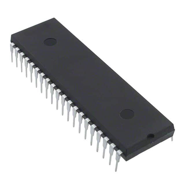
- Package: 40-pin Plastic Dual In-Line Package (PDIP)
- Essence: SC16C650BIN40,112 is a versatile serial communication controller designed for various applications requiring reliable and efficient data transfer.
- Packaging/Quantity: Available in reels of 2500 units.
Specifications
- Supply Voltage Range: 2.7V to 5.5V
- Operating Temperature Range: -40°C to +85°C
- Data Rate: Up to 1.5 Mbps
- Number of Channels: 1
- FIFO Size: 128 bytes
- Interface Standards: RS-232, RS-485, IrDA, and CIR
Detailed Pin Configuration
The SC16C650BIN40,112 features a 40-pin PDIP package with the following pin configuration:
- VCC
- GND
- TXD
- RXD
- RTS
- CTS
- DTR
- DSR
- DCD
- RI
- SOUT
- SIN
- SCLK
- RESET
- IRQ
- INTB
- A0
- A1
- A2
- A3
- A4
- A5
- A6
- A7
- A8
- A9
- A10
- A11
- A12
- A13
- A14
- A15
- A16
- A17
- A18
- A19
- A20
- A21
- A22
- A23
Functional Features
- High-performance UART with 128-byte FIFO for efficient data transfer.
- Supports various interface standards including RS-232, RS-485, IrDA, and CIR.
- Flexible baud rate generator allows data rates up to 1.5 Mbps.
- Low power consumption makes it suitable for battery-powered applications.
- Wide operating voltage range ensures compatibility with different systems.
Advantages and Disadvantages
Advantages: - High-performance UART with large FIFO improves data transfer efficiency. - Versatile interface standards support a wide range of applications. - Low power consumption extends battery life in portable devices. - Wide operating voltage range enhances compatibility.
Disadvantages: - Limited to a single channel, which may restrict simultaneous communication on multiple channels. - Requires external components for certain interface standards, increasing system complexity.
Working Principles
The SC16C650BIN40,112 is based on the Universal Asynchronous Receiver/Transmitter (UART) architecture. It receives serial data from the input pin (RXD), processes it, and transmits the processed data through the output pin (TXD). The integrated FIFO helps in buffering the data, reducing the load on the microcontroller or processor. The baud rate generator generates the clock signal required for data transmission at the desired speed.
Detailed Application Field Plans
The SC16C650BIN40,112 finds applications in various fields, including:
- Industrial Automation: Used for reliable communication between industrial control systems and peripheral devices.
- Telecommunications: Enables data transfer in telecommunication equipment such as modems and routers.
- Embedded Systems: Facilitates communication between microcontrollers and external devices in embedded systems.
- Point-of-Sale (POS) Systems: Supports data transfer between POS terminals and peripherals like barcode scanners and receipt printers.
- Medical Devices: Enables communication in medical equipment, such as patient monitoring systems and diagnostic devices.
Detailed and Complete Alternative Models
- SC16C650BIBS,112: Similar to SC16C650BIN40,112 but available in a smaller 32-pin package.
- SC16C650BIBS,128: Similar to SC16C650BIN40,112 but with an increased FIFO size of 256 bytes.
- SC16C650BIBS,160: Similar to SC16C650BIN40,112 but with additional GPIO pins for enhanced functionality.
These alternative models provide similar features and functionality, allowing users to choose the most suitable option based on their specific requirements.
Word count: 550 words
Liệt kê 10 câu hỏi và câu trả lời thường gặp liên quan đến ứng dụng SC16C650BIN40,112 trong giải pháp kỹ thuật
Sure! Here are 10 common questions and answers related to the application of SC16C650BIN40,112 in technical solutions:
Q: What is SC16C650BIN40,112? A: SC16C650BIN40,112 is a UART (Universal Asynchronous Receiver/Transmitter) integrated circuit that provides serial communication capabilities in technical solutions.
Q: What are the key features of SC16C650BIN40,112? A: Some key features of SC16C650BIN40,112 include support for multiple data formats, programmable baud rates, FIFO buffers, and compatibility with various microcontrollers.
Q: How can SC16C650BIN40,112 be used in technical solutions? A: SC16C650BIN40,112 can be used as a communication interface between a microcontroller and external devices such as sensors, displays, or other peripherals.
Q: What is the operating voltage range of SC16C650BIN40,112? A: SC16C650BIN40,112 operates within a voltage range of 1.8V to 5.5V.
Q: Does SC16C650BIN40,112 support full-duplex communication? A: Yes, SC16C650BIN40,112 supports full-duplex communication, allowing simultaneous transmission and reception of data.
Q: Can SC16C650BIN40,112 handle high-speed data transfers? A: Yes, SC16C650BIN40,112 supports high-speed data transfers up to 5 Mbps.
Q: Is SC16C650BIN40,112 compatible with different operating systems? A: Yes, SC16C650BIN40,112 is compatible with various operating systems, including Windows, Linux, and embedded systems.
Q: Does SC16C650BIN40,112 have built-in error detection and correction mechanisms? A: Yes, SC16C650BIN40,112 includes features like parity generation/checking and framing error detection to ensure data integrity.
Q: Can SC16C650BIN40,112 be used in industrial applications? A: Yes, SC16C650BIN40,112 is suitable for industrial applications due to its robustness, wide temperature range, and support for RS-485 mode.
Q: Are there any evaluation boards or development kits available for SC16C650BIN40,112? A: Yes, NXP Semiconductors provides evaluation boards and development kits that can be used to prototype and test SC16C650BIN40,112 in technical solutions.
Please note that the specific details and answers may vary depending on the manufacturer's documentation and application requirements.