

Xem thông số kỹ thuật để biết chi tiết sản phẩm.
Encyclopedia Entry: 74ACT16374SSCX
Product Information Overview
- Category: Integrated Circuit (IC)
- Use: Data Storage and Transfer
- Characteristics: High-speed, Low-power, D-type Flip-Flop
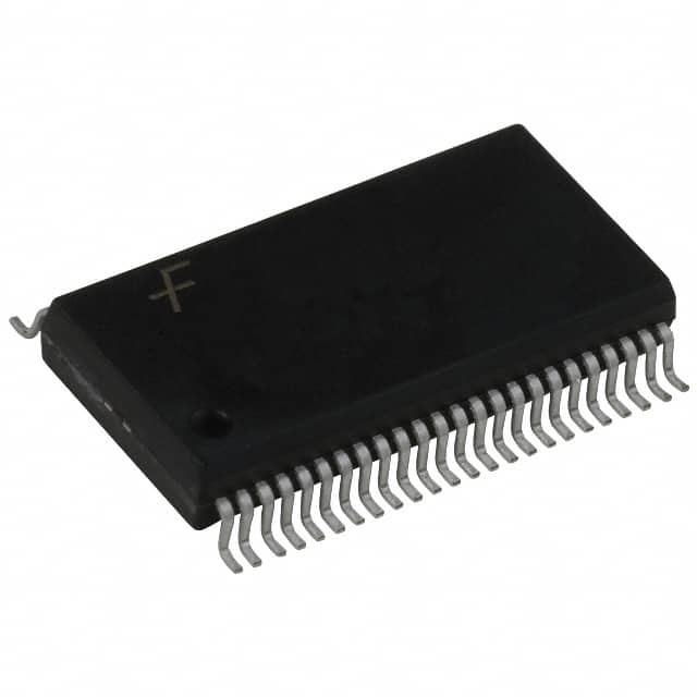
- Package: SSOP (Shrink Small Outline Package)
- Essence: Sequential Logic Device
- Packaging/Quantity: Tape and Reel, 2500 units per reel
Specifications
The 74ACT16374SSCX is a high-performance, low-power, 16-bit D-type flip-flop integrated circuit. It operates on a supply voltage range of 2.0V to 5.5V, making it suitable for various applications. The IC features a wide operating temperature range of -40°C to +85°C, ensuring reliable performance in diverse environments.
Detailed Pin Configuration
The 74ACT16374SSCX has a total of 48 pins, arranged in a SSOP package. The pin configuration is as follows:
- Pin 1: Output Q0
- Pin 2: Output Q1
- Pin 3: Output Q2
- Pin 4: Output Q3
- Pin 5: Output Q4
- Pin 6: Output Q5
- Pin 7: Output Q6
- Pin 8: Output Q7
- Pin 9: Output Q8
- Pin 10: Output Q9
- Pin 11: Output Q10
- Pin 12: Output Q11
- Pin 13: Output Q12
- Pin 14: Output Q13
- Pin 15: Output Q14
- Pin 16: Output Q15
- Pin 17: GND (Ground)
- Pin 18: Output Q15 (Complementary)
- Pin 19: Output Q14 (Complementary)
- Pin 20: Output Q13 (Complementary)
- Pin 21: Output Q12 (Complementary)
- Pin 22: Output Q11 (Complementary)
- Pin 23: Output Q10 (Complementary)
- Pin 24: Output Q9 (Complementary)
- Pin 25: Output Q8 (Complementary)
- Pin 26: Output Q7 (Complementary)
- Pin 27: Output Q6 (Complementary)
- Pin 28: Output Q5 (Complementary)
- Pin 29: Output Q4 (Complementary)
- Pin 30: Output Q3 (Complementary)
- Pin 31: Output Q2 (Complementary)
- Pin 32: Output Q1 (Complementary)
- Pin 33: Output Q0 (Complementary)
- Pin 34: GND (Ground)
- Pin 35: Clock Input (CP)
- Pin 36: Clock Enable Input (CE)
- Pin 37: Master Reset Input (MR)
- Pin 38: Data Input (D0)
- Pin 39: Data Input (D1)
- Pin 40: Data Input (D2)
- Pin 41: Data Input (D3)
- Pin 42: Data Input (D4)
- Pin 43: Data Input (D5)
- Pin 44: Data Input (D6)
- Pin 45: Data Input (D7)
- Pin 46: Data Input (D8)
- Pin 47: Data Input (D9)
- Pin 48: VCC (Supply Voltage)
Functional Features
The 74ACT16374SSCX is designed to store and transfer data in sequential logic circuits. It offers the following functional features:
- High-speed operation: The IC can operate at high clock frequencies, enabling rapid data transfer.
- Low-power consumption: It is optimized for low power usage, making it suitable for battery-powered devices.
- Wide operating voltage range: The IC can function within a wide voltage range, providing flexibility in various applications.
- Output polarity control: The complementary outputs allow for flexible signal inversion.
Advantages and Disadvantages
Advantages: - High-speed operation enables efficient data transfer. - Low-power consumption prolongs battery life in portable devices. - Wide operating voltage range allows for versatile applications. - Output polarity control provides flexibility in circuit design.
Disadvantages: - Limited number of available pins may restrict complex circuit designs. - SSOP package may require specialized equipment for soldering and handling.
Working Principles
The 74ACT16374SSCX operates based on D-type flip-flop principles. It stores and transfers data using clock signals and input data. When the clock enable (CE)
Liệt kê 10 câu hỏi và câu trả lời thường gặp liên quan đến ứng dụng 74ACT16374SSCX trong giải pháp kỹ thuật
Sure! Here are 10 common questions and answers related to the application of 74ACT16374SSCX in technical solutions:
Q: What is the 74ACT16374SSCX? A: The 74ACT16374SSCX is a 16-bit D-type flip-flop with 3-state outputs, commonly used in digital circuits.
Q: What are the key features of the 74ACT16374SSCX? A: Some key features include high-speed operation, 3-state outputs, wide operating voltage range, and compatibility with TTL input levels.
Q: How can I use the 74ACT16374SSCX in my circuit? A: You can use it as a storage element or for data transfer between different parts of your circuit.
Q: What is the maximum operating frequency of the 74ACT16374SSCX? A: The maximum operating frequency is typically specified by the manufacturer and can vary, but it is usually in the range of several hundred megahertz.
Q: Can I connect multiple 74ACT16374SSCX devices together? A: Yes, you can connect multiple devices together to increase the number of flip-flops or create larger storage registers.
Q: How do I control the 3-state outputs of the 74ACT16374SSCX? A: The 3-state outputs can be controlled using an enable signal. When the enable signal is active, the outputs are enabled, and when it is inactive, the outputs are in a high-impedance state.
Q: What is the power supply voltage range for the 74ACT16374SSCX? A: The power supply voltage range is typically specified by the manufacturer and can vary, but it is usually around 2V to 6V.
Q: Can I use the 74ACT16374SSCX in both digital and analog circuits? A: No, the 74ACT16374SSCX is designed for digital circuits and is not suitable for use in analog applications.
Q: Are there any specific precautions I need to take when using the 74ACT16374SSCX? A: It is important to follow the manufacturer's datasheet and guidelines for proper handling, power supply decoupling, and signal integrity considerations.
Q: Where can I find more information about the 74ACT16374SSCX? A: You can refer to the manufacturer's datasheet, application notes, or online resources for detailed information about the 74ACT16374SSCX and its various applications.