

Xem thông số kỹ thuật để biết chi tiết sản phẩm.
Encyclopedia Entry: 74F588PC
Product Overview
Category
The 74F588PC belongs to the category of integrated circuits (ICs), specifically a type of digital logic circuit.
Use
This IC is commonly used in electronic devices for various applications, including data processing, signal transmission, and control systems.
Characteristics
- The 74F588PC is a high-speed, low-power consumption IC.
- It operates on a wide voltage range, typically between 2V and 6V.
- This IC has multiple input and output pins, allowing for versatile connectivity.
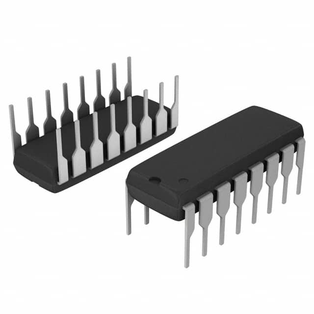
Package
The 74F588PC is available in a standard dual in-line package (DIP) format. The DIP package provides ease of installation and compatibility with existing circuit boards.
Essence
The essence of the 74F588PC lies in its ability to process digital signals efficiently and reliably, enabling seamless integration within electronic systems.
Packaging/Quantity
The 74F588PC is typically packaged in tubes or trays, containing multiple units per package. The exact quantity may vary depending on the supplier.
Specifications
- Supply Voltage Range: 2V - 6V
- Operating Temperature Range: -40°C to +85°C
- Logic Family: 74F
- Number of Pins: 20
- Input/Output Compatibility: TTL (Transistor-Transistor Logic)
- Maximum Clock Frequency: 100 MHz
Detailed Pin Configuration
The 74F588PC features 20 pins, each serving a specific function within the circuit. The pin configuration is as follows:
- Pin 1: Output A
- Pin 2: Output B
- Pin 3: Output C
- Pin 4: Output D
- Pin 5: Output E
- Pin 6: Output F
- Pin 7: Output G
- Pin 8: Output H
- Pin 9: Ground (GND)
- Pin 10: Input A
- Pin 11: Input B
- Pin 12: Input C
- Pin 13: Input D
- Pin 14: Input E
- Pin 15: Input F
- Pin 16: Input G
- Pin 17: Input H
- Pin 18: Clock Input
- Pin 19: Enable Input
- Pin 20: VCC (Power Supply)
Functional Features
The 74F588PC offers the following functional features:
- Parallel-to-Serial Conversion: It can convert parallel data inputs into a serial output stream.
- Shift Register Operation: The IC can shift data through its internal registers, allowing for sequential data processing.
- Latch Functionality: It can latch the input data and hold it until a new set of data is received.
- Clock Control: The clock input determines the timing of data transfer and synchronization.
Advantages and Disadvantages
Advantages
- High-speed operation enables rapid data processing.
- Low power consumption contributes to energy efficiency.
- Versatile input/output compatibility allows for easy integration with various systems.
- Compact DIP package facilitates installation and replacement.
Disadvantages
- Limited number of input/output pins may restrict complex circuit designs.
- Sensitivity to voltage fluctuations may require additional voltage regulation measures.
Working Principles
The 74F588PC operates based on the principles of digital logic circuits. It utilizes a combination of flip-flops, shift registers, and latches to process and manipulate digital signals. The clock input controls the timing of data transfer, while the enable input determines when the IC is active.
Detailed Application Field Plans
The 74F588PC finds applications in various fields, including:
- Data Communication Systems: It can be used for data serialization and deserialization in communication protocols.
- Industrial Control Systems: The IC enables efficient control signal processing in automation and robotics.
- Display Technologies: It can drive LED displays and control pixel data transmission in visual display systems.
- Memory Addressing: The IC can be employed for address decoding and multiplexing in memory systems.
Detailed and Complete Alternative Models
There are several alternative models available that offer similar functionality to the 74F588PC. Some notable alternatives include:
- 74HC595: A CMOS-based shift register with similar pin configuration and functionality.
- CD4021: A parallel-to-serial shift register IC with additional features like serial output cascade capability.
- SN74LS164: A TTL-compatible shift register with parallel input and serial output capabilities.
These alternative models provide options for different voltage ranges, package types, and specific application requirements.
In conclusion, the 74F588PC is a versatile integrated circuit that excels in digital signal processing and manipulation. Its high-speed operation, low power consumption, and compact
Liệt kê 10 câu hỏi và câu trả lời thường gặp liên quan đến ứng dụng 74F588PC trong giải pháp kỹ thuật
Sure! Here are 10 common questions and answers related to the application of 74F588PC in technical solutions:
Q: What is the 74F588PC? A: The 74F588PC is a 8-bit universal shift/storage register with three-state outputs, commonly used in digital circuits.
Q: What are the key features of the 74F588PC? A: The key features include 8-bit parallel-in/serial-out shifting, three-state outputs, asynchronous master reset, and high-speed operation.
Q: How can I use the 74F588PC in my circuit? A: You can use it for serial-to-parallel or parallel-to-serial data conversion, data storage, data transfer between systems, and other applications requiring shift registers.
Q: What is the maximum clock frequency supported by the 74F588PC? A: The 74F588PC can operate at a maximum clock frequency of typically 100 MHz.
Q: Can I cascade multiple 74F588PCs together? A: Yes, you can cascade multiple 74F588PCs to increase the number of bits in your shift register.
Q: How do I connect the inputs and outputs of the 74F588PC? A: The inputs (parallel data inputs, clock, and reset) and outputs (serial output and three-state outputs) should be connected according to the datasheet's recommended pin configuration.
Q: What is the power supply voltage range for the 74F588PC? A: The 74F588PC operates with a power supply voltage range of typically 4.5V to 5.5V.
Q: Can I use the 74F588PC in both TTL and CMOS logic systems? A: Yes, the 74F588PC is compatible with both TTL and CMOS logic systems.
Q: Are there any specific precautions I should take while using the 74F588PC? A: It is important to ensure proper decoupling capacitors are used near the power supply pins, and to follow the recommended operating conditions mentioned in the datasheet.
Q: Where can I find more detailed information about the 74F588PC? A: You can refer to the datasheet provided by the manufacturer, which contains detailed information about the electrical characteristics, pin configuration, and recommended usage of the 74F588PC.
Please note that the answers provided here are general and may vary depending on the specific application and requirements.