

Xem thông số kỹ thuật để biết chi tiết sản phẩm.
74LVTH240MTC
Product Overview
Category
The 74LVTH240MTC belongs to the category of integrated circuits (ICs).
Use
This IC is commonly used for signal amplification and buffering in digital electronic circuits.
Characteristics
- High-speed operation
- Low power consumption
- Wide operating voltage range
- Compatibility with various logic families
- Schmitt trigger inputs for noise immunity
Package
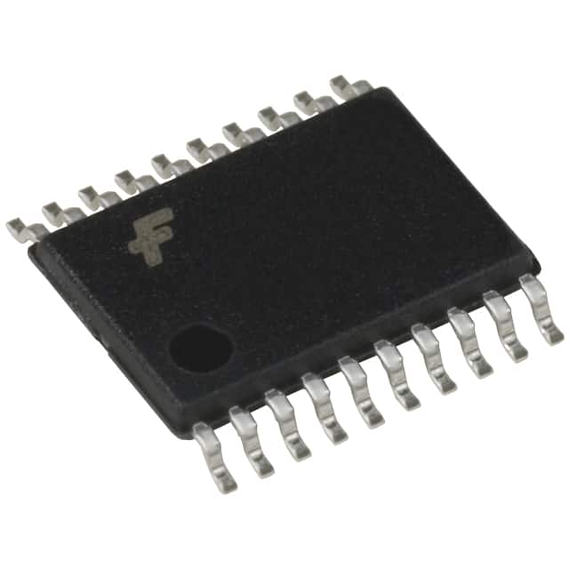
The 74LVTH240MTC is available in a small outline package (SOIC) with 20 pins.
Essence
The essence of the 74LVTH240MTC lies in its ability to amplify and buffer digital signals, ensuring reliable transmission within electronic circuits.
Packaging/Quantity
The 74LVTH240MTC is typically packaged in reels or tubes, with quantities varying depending on the supplier.
Specifications
- Supply Voltage: 2.0V to 5.5V
- Input Voltage: 0V to VCC
- Output Voltage: 0V to VCC
- Operating Temperature Range: -40°C to +85°C
- Input Capacitance: 3.5pF (typical)
- Output Capacitance: 6pF (typical)
- Propagation Delay Time: 4.1ns (typical)
Detailed Pin Configuration
The 74LVTH240MTC has a total of 20 pins, which are assigned specific functions as follows:
- A1: Input A1
- Y1: Output Y1
- A2: Input A2
- Y2: Output Y2
- GND: Ground
- A3: Input A3
- Y3: Output Y3
- A4: Input A4
- Y4: Output Y4
- GND: Ground
- OE: Output Enable
- Y5: Output Y5
- A5: Input A5
- Y6: Output Y6
- A6: Input A6
- Y7: Output Y7
- VCC: Power Supply
- A7: Input A7
- Y8: Output Y8
- A8: Input A8
Functional Features
- Signal amplification and buffering
- High-speed operation for efficient data transmission
- Schmitt trigger inputs for noise immunity
- Wide operating voltage range allows compatibility with various logic families
- Low power consumption for energy-efficient designs
Advantages and Disadvantages
Advantages
- High-speed operation enables fast data processing
- Low power consumption helps conserve energy
- Wide operating voltage range allows for compatibility with different systems
- Schmitt trigger inputs provide noise immunity, ensuring reliable signal transmission
Disadvantages
- Limited number of input/output channels (8 in total)
- May require additional components for complex circuit designs
Working Principles
The 74LVTH240MTC operates by receiving digital signals at its input pins (A1-A8) and amplifying/buffering them to the corresponding output pins (Y1-Y8). The output enable pin (OE) controls the activation of the outputs. When the OE pin is low, the outputs are enabled, allowing the amplified signals to pass through. Conversely, when the OE pin is high, the outputs are disabled, resulting in no signal transmission.
Detailed Application Field Plans
The 74LVTH240MTC finds applications in various fields, including:
- Microprocessor-based systems
- Data communication networks
- Industrial automation
- Automotive electronics
- Consumer electronics
In microprocessor-based systems, this IC can be used for address and data bus buffering, ensuring reliable communication between the microprocessor and other peripheral devices. In data communication networks, it can serve as a signal amplifier to enhance signal integrity during transmission. In industrial automation and automotive electronics, the 74LVTH240MTC can be utilized for signal buffering and level shifting in control systems. Lastly, in consumer electronics, it can be employed for signal amplification in audio/video equipment.
Detailed and Complete Alternative Models
- SN74LVTH240: Similar IC from Texas Instruments
- MC74LVTH240: Equivalent IC from ON Semiconductor
- CD74LVTH240: Alternative IC from Texas Instruments
- 74HCT240: Compatible IC from various manufacturers
These alternative models offer similar functionality and characteristics to the 74LVTH240MTC, providing users with options based on availability and specific requirements.
Word count: 607 words
Liệt kê 10 câu hỏi và câu trả lời thường gặp liên quan đến ứng dụng 74LVTH240MTC trong giải pháp kỹ thuật
Sure! Here are 10 common questions and answers related to the application of 74LVTH240MTC in technical solutions:
Q: What is the 74LVTH240MTC?
- A: The 74LVTH240MTC is a 3.3V octal buffer/line driver with 3-state outputs.
Q: What is the maximum operating voltage for the 74LVTH240MTC?
- A: The maximum operating voltage for the 74LVTH240MTC is 3.6V.
Q: How many inputs and outputs does the 74LVTH240MTC have?
- A: The 74LVTH240MTC has 8 inputs and 8 outputs.
Q: Can the 74LVTH240MTC be used as a level shifter?
- A: Yes, the 74LVTH240MTC can be used as a level shifter between different voltage domains.
Q: What is the output current capability of the 74LVTH240MTC?
- A: The 74LVTH240MTC has a typical output current capability of ±24mA.
Q: Is the 74LVTH240MTC compatible with TTL logic levels?
- A: Yes, the 74LVTH240MTC is compatible with both TTL and CMOS logic levels.
Q: Can the 74LVTH240MTC be used in high-speed applications?
- A: Yes, the 74LVTH240MTC is designed for high-speed operation and has a propagation delay of only a few nanoseconds.
Q: Does the 74LVTH240MTC have built-in protection against electrostatic discharge (ESD)?
- A: Yes, the 74LVTH240MTC has built-in ESD protection to prevent damage from static electricity.
Q: Can the 74LVTH240MTC be used in both input and output buffer applications?
- A: Yes, the 74LVTH240MTC can be used as both an input buffer and an output buffer in various applications.
Q: What is the package type of the 74LVTH240MTC?
- A: The 74LVTH240MTC is available in a TSSOP (Thin Shrink Small Outline Package) package.
Please note that these answers are general and may vary depending on the specific datasheet and manufacturer's specifications for the 74LVTH240MTC.