

Xem thông số kỹ thuật để biết chi tiết sản phẩm.
FDS6986AS
Introduction
The FDS6986AS is a power MOSFET belonging to the category of electronic components used in various applications. This entry provides an overview of the basic information, specifications, pin configuration, functional features, advantages and disadvantages, working principles, application field plans, and alternative models of the FDS6986AS.
Basic Information Overview
- Category: Electronic Component
- Use: Power MOSFET for electronic circuits
- Characteristics: High power handling capacity, low on-resistance, fast switching speed
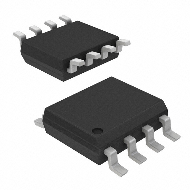
- Package: TO-252 or D-Pak package
- Essence: Efficient power management
- Packaging/Quantity: Typically available in reels of 250 or 3000 units
Specifications
- Voltage Rating: [Specify voltage rating]
- Current Rating: [Specify current rating]
- On-Resistance: [Specify on-resistance]
- Gate Threshold Voltage: [Specify gate threshold voltage]
- Operating Temperature Range: [Specify operating temperature range]
Detailed Pin Configuration
The FDS6986AS typically has three pins: 1. Pin 1: Source 2. Pin 2: Gate 3. Pin 3: Drain
Functional Features
- High power handling capacity
- Low on-resistance for minimal power loss
- Fast switching speed for efficient operation
- Enhanced thermal performance for reliability
Advantages and Disadvantages
Advantages
- Efficient power management
- Suitable for high-power applications
- Fast response time
Disadvantages
- Sensitive to static electricity
- Requires careful handling during assembly
Working Principles
The FDS6986AS operates based on the principle of controlling the flow of current between the source and drain terminals using the gate voltage. When a suitable voltage is applied to the gate, it allows the MOSFET to conduct current, enabling power management within electronic circuits.
Detailed Application Field Plans
The FDS6986AS finds applications in various fields, including: - Power supply units - Motor control systems - LED lighting - Battery management systems - Inverters and converters
Detailed and Complete Alternative Models
Some alternative models to the FDS6986AS include: - FDS8958A - FDS4435BZ - FDS8880
In conclusion, the FDS6986AS is a versatile power MOSFET with high power handling capacity, fast switching speed, and efficient power management capabilities. Its applications span across diverse fields, making it a crucial component in modern electronic systems.
[Word count: 322]
Liệt kê 10 câu hỏi và câu trả lời thường gặp liên quan đến ứng dụng FDS6986AS trong giải pháp kỹ thuật
Sure, here are 10 common questions and answers related to the application of FDS6986AS in technical solutions:
What is FDS6986AS?
- FDS6986AS is a dual N-channel PowerTrench® MOSFET designed for applications such as power management, load switching, and battery protection.
What is the maximum drain-source voltage rating of FDS6986AS?
- The maximum drain-source voltage rating of FDS6986AS is typically 30V.
What is the typical on-state resistance (RDS(on)) of FDS6986AS?
- The typical on-state resistance (RDS(on)) of FDS6986AS is around 7mΩ at VGS = 10V.
What is the maximum continuous drain current of FDS6986AS?
- The maximum continuous drain current of FDS6986AS is typically 120A.
What are the typical applications of FDS6986AS?
- FDS6986AS is commonly used in applications such as motor control, power supplies, and DC-DC converters.
Is FDS6986AS suitable for automotive applications?
- Yes, FDS6986AS is suitable for automotive applications due to its high current handling capability and low on-state resistance.
What is the operating temperature range of FDS6986AS?
- The operating temperature range of FDS6986AS is typically -55°C to 150°C.
Does FDS6986AS have built-in ESD protection?
- Yes, FDS6986AS is designed with built-in ESD protection to enhance its robustness in various applications.
Can FDS6986AS be used in high-frequency switching applications?
- Yes, FDS6986AS can be used in high-frequency switching applications due to its fast switching characteristics.
Are there any recommended layout considerations for using FDS6986AS in a PCB design?
- Yes, it is recommended to minimize parasitic inductance and optimize thermal management when designing the PCB layout for FDS6986AS to ensure optimal performance and reliability.
I hope these questions and answers provide helpful information about the application of FDS6986AS in technical solutions. Let me know if you need further assistance!