

Xem thông số kỹ thuật để biết chi tiết sản phẩm.
NB100LVEP56MN
Basic Information Overview
- Category: Integrated Circuit (IC)
- Use: Signal transmission and reception in high-speed digital communication systems
- Characteristics:
- High-speed operation
- Low voltage differential signaling (LVDS) technology
- Small form factor
- Low power consumption
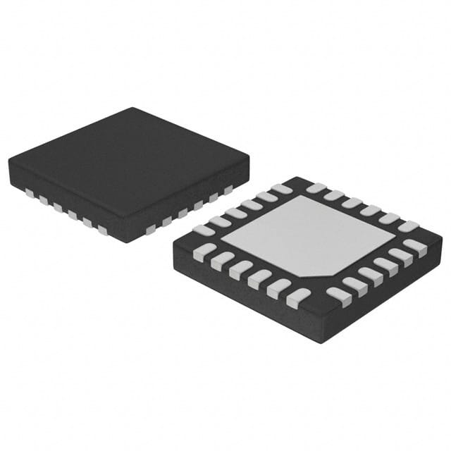
- Package: Surface Mount Technology (SMT) package
- Essence: Efficient signal transmission and reception in high-speed digital communication systems
- Packaging/Quantity: Available in reels or trays, quantity depends on supplier
Specifications
- Supply Voltage: 3.3V
- Input Voltage Range: 0V to VCC
- Output Voltage Range: 0V to VCC
- Operating Temperature Range: -40°C to +85°C
- Data Rate: Up to 1.5 Gbps
- Number of Pins: 56
Detailed Pin Configuration
The NB100LVEP56MN IC has a total of 56 pins. The pin configuration is as follows:
- Pin 1: VCC
- Pin 2: GND
- Pin 3: LVDS_OUT0
- Pin 4: LVDS_OUT0B
- Pin 5: LVDS_OUT1
- Pin 6: LVDS_OUT1B
- Pin 7: LVDS_OUT2
- Pin 8: LVDS_OUT2B
- Pin 9: LVDS_OUT3
- Pin 10: LVDS_OUT3B
- Pin 11: LVDS_OUT4
- Pin 12: LVDS_OUT4B
- Pin 13: LVDS_OUT5
- Pin 14: LVDS_OUT5B
- Pin 15: LVDS_OUT6
- Pin 16: LVDS_OUT6B
- Pin 17: LVDS_OUT7
- Pin 18: LVDS_OUT7B
- Pin 19: LVDS_OUT8
- Pin 20: LVDS_OUT8B
- Pin 21: LVDS_OUT9
- Pin 22: LVDS_OUT9B
- Pin 23: LVDS_OUT10
- Pin 24: LVDS_OUT10B
- Pin 25: LVDS_OUT11
- Pin 26: LVDS_OUT11B
- Pin 27: LVDS_OUT12
- Pin 28: LVDS_OUT12B
- Pin 29: LVDS_OUT13
- Pin 30: LVDS_OUT13B
- Pin 31: LVDS_OUT14
- Pin 32: LVDS_OUT14B
- Pin 33: LVDS_OUT15
- Pin 34: LVDS_OUT15B
- Pin 35: LVDS_OUT16
- Pin 36: LVDS_OUT16B
- Pin 37: LVDS_OUT17
- Pin 38: LVDS_OUT17B
- Pin 39: LVDS_OUT18
- Pin 40: LVDS_OUT18B
- Pin 41: LVDS_OUT19
- Pin 42: LVDS_OUT19B
- Pin 43: LVDS_OUT20
- Pin 44: LVDS_OUT20B
- Pin 45: LVDS_OUT21
- Pin 46: LVDS_OUT21B
- Pin 47: LVDS_OUT22
- Pin 48: LVDS_OUT22B
- Pin 49: LVDS_OUT23
- Pin 50: LVDS_OUT23B
- Pin 51: LVDS_OUT24
- Pin 52: LVDS_OUT24B
- Pin 53: LVDS_OUT25
- Pin 54: LVDS_OUT25B
- Pin 55: LVDS_OUT26
- Pin 56: LVDS_OUT26B
Functional Features
- High-speed signal transmission and reception
- Low voltage differential signaling (LVDS) technology for noise immunity
- Wide operating temperature range
- Small form factor for space-constrained applications
- Low power consumption for energy efficiency
Advantages and Disadvantages
Advantages: - High-speed operation enables efficient data transfer - LVDS technology provides noise immunity and reliable signal integrity - Small form factor allows for compact system designs - Low power consumption reduces energy usage
Disadvantages: - Requires careful PCB layout and signal routing for optimal performance - Limited number of pins may restrict the complexity of the system design
Working Principles
The NB100LVEP56MN IC operates based on LVDS technology
Liệt kê 10 câu hỏi và câu trả lời thường gặp liên quan đến ứng dụng NB100LVEP56MN trong giải pháp kỹ thuật
Sure! Here are 10 common questions and answers related to the application of NB100LVEP56MN in technical solutions:
Q: What is NB100LVEP56MN? A: NB100LVEP56MN is a high-speed differential receiver designed for applications requiring low skew and high data rates.
Q: What is the maximum data rate supported by NB100LVEP56MN? A: NB100LVEP56MN supports data rates up to 3.2 Gbps, making it suitable for high-speed communication systems.
Q: What is the operating voltage range of NB100LVEP56MN? A: NB100LVEP56MN operates with a supply voltage range of 2.375V to 3.8V.
Q: Can NB100LVEP56MN be used in both single-ended and differential applications? A: No, NB100LVEP56MN is specifically designed for differential signaling applications.
Q: What is the typical propagation delay of NB100LVEP56MN? A: The typical propagation delay of NB100LVEP56MN is around 200 ps.
Q: Does NB100LVEP56MN support AC-coupled inputs? A: Yes, NB100LVEP56MN supports AC-coupled inputs, which allows for easy integration with different signal sources.
Q: Can NB100LVEP56MN operate in a wide temperature range? A: Yes, NB100LVEP56MN has an extended temperature range from -40°C to +85°C, making it suitable for various environments.
Q: What is the output swing of NB100LVEP56MN? A: The output swing of NB100LVEP56MN is typically 800 mV, which ensures compatibility with other devices.
Q: Does NB100LVEP56MN have built-in termination resistors? A: No, NB100LVEP56MN does not have built-in termination resistors. External termination resistors are required for proper signal integrity.
Q: What package options are available for NB100LVEP56MN? A: NB100LVEP56MN is available in a small footprint 32-pin QFN package, which offers ease of integration and space-saving benefits.
Please note that these answers are general and may vary depending on the specific datasheet and manufacturer's specifications for NB100LVEP56MN.