

Xem thông số kỹ thuật để biết chi tiết sản phẩm.
NC7SZ126P5X
Product Overview
- Category: Integrated Circuit (IC)
- Use: Logic Gate
- Characteristics: Single Buffer/Driver, Non-Inverting, 3-State Output
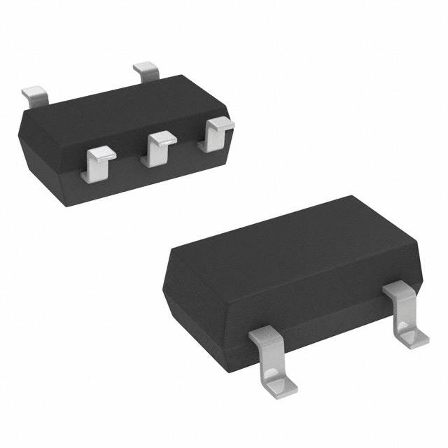
- Package: SC-70-5
- Essence: High-Speed CMOS Technology
- Packaging/Quantity: Tape and Reel, 3000 pieces per reel
Specifications
- Supply Voltage Range: 1.65V to 5.5V
- Input Voltage Range: 0V to VCC
- Output Voltage Range: 0V to VCC
- Operating Temperature Range: -40°C to +85°C
- Propagation Delay Time: 2.5ns (typical)
- Maximum Quiescent Current: 10μA
Detailed Pin Configuration
The NC7SZ126P5X has a total of 5 pins:
- Pin 1: Input (A)
- Pin 2: Enable (EN)
- Pin 3: Output (Y)
- Pin 4: Ground (GND)
- Pin 5: Power Supply (VCC)
Functional Features
- Non-inverting buffer/driver with 3-state output
- High-speed operation due to advanced CMOS technology
- Low power consumption
- Wide supply voltage range for compatibility with various systems
- 3-state output allows multiple devices to share a common bus
Advantages and Disadvantages
Advantages
- High-speed operation enables efficient data transmission
- Low power consumption prolongs battery life in portable devices
- Wide supply voltage range ensures compatibility with different systems
- 3-state output facilitates bus sharing among multiple devices
Disadvantages
- Limited number of input/output pins restricts the complexity of circuits that can be built
- Not suitable for applications requiring high current or voltage levels
Working Principles
The NC7SZ126P5X is a logic gate that acts as a buffer/driver. It takes an input signal (A) and amplifies it to provide a non-inverted output signal (Y). The enable pin (EN) controls the output state, allowing it to be either active or in a high-impedance state.
The IC operates using high-speed CMOS technology, which ensures fast signal propagation and low power consumption. It can be powered by a supply voltage ranging from 1.65V to 5.5V, making it compatible with various systems.
Detailed Application Field Plans
The NC7SZ126P5X finds applications in various fields, including:
- Communication Systems: Used in data transmission circuits to amplify and buffer signals.
- Computers and Peripherals: Employed in interface circuits to enable communication between different components.
- Consumer Electronics: Integrated into portable devices to control signal routing and level shifting.
- Automotive Electronics: Utilized in automotive control units for signal conditioning and interfacing.
- Industrial Automation: Incorporated in control systems to drive actuators and sensors.
Detailed and Complete Alternative Models
- SN74LVC1G126DBVR: Single Buffer/Driver, Non-Inverting, 3-State Output, SOT-23-5 package.
- 74HC126D: Quad Buffer/Driver, Non-Inverting, 3-State Output, SOIC-14 package.
- CD40106BE: Hex Schmitt Trigger, Inverting, DIP-14 package.
These alternative models offer similar functionality and can be used as substitutes for the NC7SZ126P5X in various applications.
Word count: 430 words
Liệt kê 10 câu hỏi và câu trả lời thường gặp liên quan đến ứng dụng NC7SZ126P5X trong giải pháp kỹ thuật
Sure! Here are 10 common questions and answers related to the application of NC7SZ126P5X in technical solutions:
Question: What is the NC7SZ126P5X?
Answer: The NC7SZ126P5X is a single buffer gate IC (Integrated Circuit) that can be used for signal buffering and level shifting applications.Question: What is the operating voltage range of NC7SZ126P5X?
Answer: The NC7SZ126P5X operates within a voltage range of 1.65V to 5.5V.Question: Can I use NC7SZ126P5X for level shifting between different voltage domains?
Answer: Yes, the NC7SZ126P5X can be used for level shifting between different voltage domains, making it suitable for interfacing between devices with different voltage requirements.Question: What is the maximum output current of NC7SZ126P5X?
Answer: The NC7SZ126P5X has a maximum output current of 32mA.Question: Is the NC7SZ126P5X compatible with both CMOS and TTL logic levels?
Answer: Yes, the NC7SZ126P5X is compatible with both CMOS and TTL logic levels, providing flexibility in various digital circuit designs.Question: Can I use the NC7SZ126P5X for bidirectional level shifting?
Answer: No, the NC7SZ126P5X is a unidirectional buffer gate and cannot be used for bidirectional level shifting. For bidirectional level shifting, you would need a different IC or a combination of multiple gates.Question: What is the typical propagation delay of the NC7SZ126P5X?
Answer: The typical propagation delay of the NC7SZ126P5X is around 4.5ns.Question: Can I use the NC7SZ126P5X in high-speed applications?
Answer: Yes, the NC7SZ126P5X can be used in high-speed applications as it has a fast propagation delay and supports high-frequency operation.Question: Does the NC7SZ126P5X have built-in ESD protection?
Answer: Yes, the NC7SZ126P5X has built-in ESD (Electrostatic Discharge) protection, which helps protect the IC from damage due to electrostatic discharge events.Question: What package options are available for the NC7SZ126P5X?
Answer: The NC7SZ126P5X is available in various package options, including SOT-23-5 and SC-70-5, providing flexibility for different PCB layouts and space constraints.
Please note that these answers are general and may vary depending on the specific datasheet and manufacturer's specifications for the NC7SZ126P5X.