

Xem thông số kỹ thuật để biết chi tiết sản phẩm.
NCP1012ST130T3G
Basic Information Overview
- Category: Integrated Circuit (IC)
- Use: Power Management
- Characteristics: Switching Regulator Controller
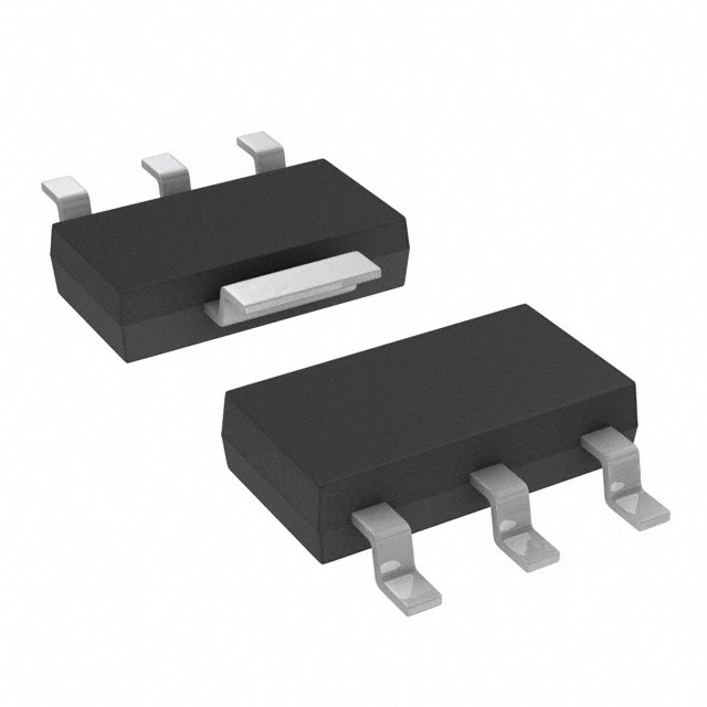
- Package: SOT-223
- Essence: High-performance, energy-efficient power management solution
- Packaging/Quantity: Tape and Reel, 2500 units per reel
Specifications
- Input Voltage Range: 7.5V to 25V
- Output Voltage Range: 4.9V to 5.1V
- Maximum Output Current: 130mA
- Operating Temperature Range: -40°C to +125°C
- Frequency Range: 65kHz to 115kHz
- Duty Cycle Range: 0% to 100%
- Standby Power Consumption: <50mW
Detailed Pin Configuration
The NCP1012ST130T3G has a total of 6 pins: 1. VCC: Power supply input pin 2. GND: Ground reference pin 3. FB: Feedback pin for output voltage regulation 4. COMP: Compensation pin for stability control 5. CS: Current sense pin for current limit protection 6. DRAIN: Switching transistor drain pin
Functional Features
- Pulse Frequency Modulation (PFM) control scheme for high efficiency
- Built-in overvoltage and undervoltage protection
- Soft-start function for smooth startup
- Overcurrent protection with automatic restart
- Low standby power consumption for energy savings
- Wide input voltage range for versatile applications
Advantages and Disadvantages
Advantages: - High-performance power management solution - Energy-efficient operation - Compact SOT-223 package for space-constrained designs - Comprehensive protection features for enhanced reliability - Wide input voltage range allows for flexible usage
Disadvantages: - Limited maximum output current may not be suitable for high-power applications - Requires external components for complete power supply design
Working Principles
The NCP1012ST130T3G is a switching regulator controller IC that utilizes Pulse Frequency Modulation (PFM) control scheme. It regulates the output voltage by adjusting the duty cycle of the switching transistor. The feedback pin (FB) monitors the output voltage and provides the necessary information to the internal control circuitry, which adjusts the duty cycle accordingly. This control scheme ensures high efficiency and stable output voltage.
Detailed Application Field Plans
The NCP1012ST130T3G is commonly used in various power management applications, including but not limited to: - Power supplies for consumer electronics - Battery chargers - LED lighting systems - Industrial automation equipment - Automotive electronics
Detailed and Complete Alternative Models
- NCP1012AP065G: Similar functionality with a different package (PDIP-7)
- NCP1012ST100T3G: Lower maximum output current (100mA) but similar features
- NCP1012ST150T3G: Higher maximum output current (150mA) but similar features
These alternative models provide flexibility in choosing the most suitable option based on specific requirements.
Word count: 386 words
Liệt kê 10 câu hỏi và câu trả lời thường gặp liên quan đến ứng dụng NCP1012ST130T3G trong giải pháp kỹ thuật
Sure! Here are 10 common questions and answers related to the application of NCP1012ST130T3G in technical solutions:
Q: What is NCP1012ST130T3G? A: NCP1012ST130T3G is a high-performance integrated circuit (IC) designed for offline flyback converters used in power supply applications.
Q: What is the input voltage range for NCP1012ST130T3G? A: The input voltage range for NCP1012ST130T3G is typically between 85V and 265V AC.
Q: What is the output power range supported by NCP1012ST130T3G? A: NCP1012ST130T3G supports an output power range of up to 12W.
Q: Can NCP1012ST130T3G be used in both isolated and non-isolated power supply designs? A: Yes, NCP1012ST130T3G can be used in both isolated and non-isolated power supply designs.
Q: What is the maximum switching frequency of NCP1012ST130T3G? A: The maximum switching frequency of NCP1012ST130T3G is typically around 130 kHz.
Q: Does NCP1012ST130T3G have built-in protection features? A: Yes, NCP1012ST130T3G has built-in protection features such as overvoltage protection (OVP), overload protection (OLP), and thermal shutdown.
Q: Can NCP1012ST130T3G operate in continuous or discontinuous conduction mode? A: NCP1012ST130T3G can operate in both continuous conduction mode (CCM) and discontinuous conduction mode (DCM).
Q: What is the typical efficiency of NCP1012ST130T3G? A: The typical efficiency of NCP1012ST130T3G is around 80-85%, depending on the specific application and operating conditions.
Q: Is NCP1012ST130T3G suitable for low-power applications? A: Yes, NCP1012ST130T3G is suitable for low-power applications as it supports output power up to 12W.
Q: Are there any reference designs available for NCP1012ST130T3G? A: Yes, ON Semiconductor provides reference designs and application notes that can help in implementing NCP1012ST130T3G in various technical solutions.
Please note that the answers provided here are general and may vary based on specific design requirements and application considerations. It is always recommended to refer to the datasheet and application notes provided by the manufacturer for detailed information.