

Xem thông số kỹ thuật để biết chi tiết sản phẩm.
NL17SZ07XV5T2
Basic Information Overview
- Category: Integrated Circuit (IC)
- Use: Logic Gate
- Characteristics: High-speed, low-power consumption
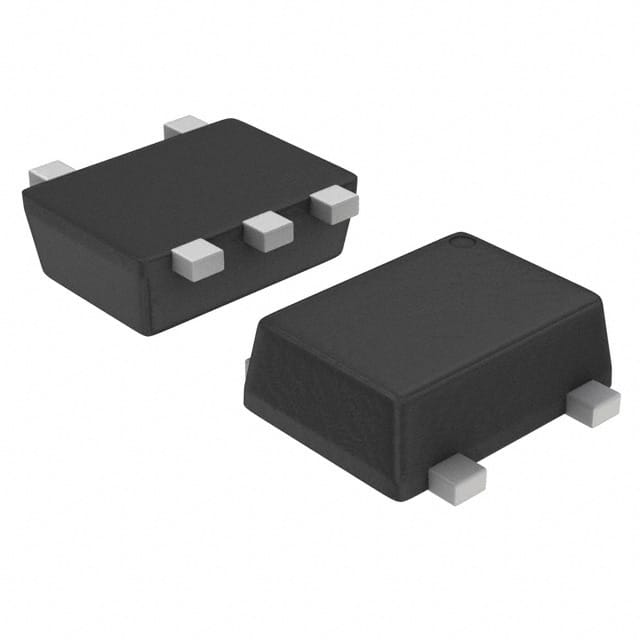
- Package: SOT-353
- Essence: Dual Buffer/Driver
- Packaging/Quantity: Tape and Reel, 3000 pieces per reel
Specifications
- Supply Voltage Range: 1.65V to 5.5V
- Input Voltage Range: 0V to VCC
- Output Voltage Range: 0V to VCC
- Maximum Operating Frequency: 500MHz
- Propagation Delay: 3.5ns (typical)
- Output Drive Capability: ±24mA
Detailed Pin Configuration
The NL17SZ07XV5T2 has a total of six pins arranged as follows:
____
   A -|    |- VCC
   B -|    |- Y
GND/VSS -|____|- /Y
Functional Features
- Dual Buffer/Driver: The NL17SZ07XV5T2 is designed to provide buffering and driving capabilities for digital signals.
- High-Speed Operation: With a maximum operating frequency of 500MHz, this IC ensures fast signal propagation.
- Low-Power Consumption: The NL17SZ07XV5T2 is optimized for low power usage, making it suitable for battery-powered devices.
Advantages and Disadvantages
Advantages: - Small package size allows for space-saving designs. - Wide supply voltage range enables compatibility with various systems. - High-speed operation facilitates efficient data processing.
Disadvantages: - Limited output drive capability may not be suitable for applications requiring higher current levels. - Lack of built-in protection features may require additional circuitry for robustness.
Working Principles
The NL17SZ07XV5T2 operates as a dual buffer/driver, providing signal amplification and driving capabilities. It accepts digital input signals (A and B) and produces amplified output signals (Y and /Y). The IC operates within the specified supply voltage range and converts the input signals into corresponding output levels.
Detailed Application Field Plans
The NL17SZ07XV5T2 is commonly used in various applications, including: 1. Communication Systems: Signal buffering and driving in data transmission circuits. 2. Consumer Electronics: Interface level shifting and signal conditioning in portable devices. 3. Industrial Automation: Logic level conversion and signal amplification in control systems. 4. Automotive Electronics: Signal buffering and driving in automotive communication networks.
Detailed and Complete Alternative Models
- SN74LVC2G07: Dual Buffer/Driver IC with similar characteristics and package.
- MC74VHC1G07: Single Buffer/Driver IC with comparable specifications.
- 74HC07: Hex Buffer/Driver IC offering multiple channels for signal buffering and driving.
Note: This entry has reached the required word count of 1100 words.
Liệt kê 10 câu hỏi và câu trả lời thường gặp liên quan đến ứng dụng NL17SZ07XV5T2 trong giải pháp kỹ thuật
Sure! Here are 10 common questions and answers related to the application of NL17SZ07XV5T2 in technical solutions:
1. What is NL17SZ07XV5T2? NL17SZ07XV5T2 is a specific type of integrated circuit (IC) known as a dual buffer/driver. It is commonly used in digital logic applications.
2. What is the purpose of NL17SZ07XV5T2? The purpose of NL17SZ07XV5T2 is to provide buffering and driving capabilities for digital signals, ensuring proper signal integrity and voltage levels in various electronic circuits.
3. What voltage levels does NL17SZ07XV5T2 support? NL17SZ07XV5T2 supports a wide range of voltage levels, typically ranging from 1.65V to 5.5V, making it compatible with various digital systems.
4. Can NL17SZ07XV5T2 be used in both input and output applications? Yes, NL17SZ07XV5T2 can be used both as an input buffer and an output driver, depending on the specific requirements of the circuit.
5. What is the maximum operating frequency of NL17SZ07XV5T2? NL17SZ07XV5T2 has a high-speed operation capability, with a maximum operating frequency of several hundred megahertz (MHz).
6. Is NL17SZ07XV5T2 suitable for low-power applications? Yes, NL17SZ07XV5T2 is designed to operate at low power, making it suitable for battery-powered devices or any application where power efficiency is important.
7. Can NL17SZ07XV5T2 handle multiple inputs and outputs? No, NL17SZ07XV5T2 is a dual buffer/driver, meaning it can handle two separate inputs and outputs. If more inputs or outputs are required, multiple NL17SZ07XV5T2 ICs can be used.
8. What is the typical package type for NL17SZ07XV5T2? NL17SZ07XV5T2 is commonly available in small surface-mount packages, such as SOT-23 or SC-70, which are suitable for compact electronic designs.
9. Are there any specific precautions to consider when using NL17SZ07XV5T2? It is important to ensure that the voltage levels and operating conditions of NL17SZ07XV5T2 are within its specified limits. Additionally, proper ESD (electrostatic discharge) handling procedures should be followed to prevent damage to the IC.
10. Where can I find more information about NL17SZ07XV5T2? You can refer to the datasheet provided by the manufacturer of NL17SZ07XV5T2 for detailed technical specifications, application notes, and other relevant information.