

Xem thông số kỹ thuật để biết chi tiết sản phẩm.
NL17SZ17XV5T2G
Basic Information Overview
- Category: Integrated Circuit (IC)
- Use: Logic Gate
- Characteristics: High-speed, Low-power consumption
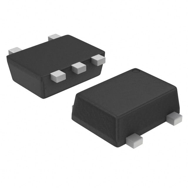
- Package: SOT-353
- Essence: Single Schmitt-Trigger Inverter
- Packaging/Quantity: Tape and Reel / 3000 units per reel
Specifications
- Supply Voltage Range: 1.65V to 5.5V
- Input Voltage Range: 0V to VCC
- Output Voltage Range: 0V to VCC
- Operating Temperature Range: -40°C to +85°C
- Propagation Delay Time: 3.5ns (typical)
- Maximum Quiescent Current: 1μA (at 5.5V)
Detailed Pin Configuration
The NL17SZ17XV5T2G has a total of 5 pins: 1. Pin 1: Input (A) 2. Pin 2: Ground (GND) 3. Pin 3: Output (Y) 4. Pin 4: Power Supply (VCC) 5. Pin 5: Input (B)
Functional Features
- Single Schmitt-Trigger Inverter with hysteresis
- Provides noise immunity and signal conditioning
- Converts slowly changing input signals into sharply defined output signals
- Suitable for high-speed digital applications
- Low-power consumption makes it ideal for battery-operated devices
Advantages
- High-speed operation allows for efficient signal processing
- Low-power consumption extends battery life in portable devices
- Noise immunity ensures reliable signal transmission
- Small package size saves board space in compact designs
- Wide supply voltage range enhances compatibility with various systems
Disadvantages
- Limited number of inputs and outputs restricts complex circuit designs
- Hysteresis may introduce additional delay in signal propagation
- Sensitivity to voltage fluctuations may affect performance in unstable power conditions
Working Principles
The NL17SZ17XV5T2G is a Single Schmitt-Trigger Inverter, which means it utilizes hysteresis to provide noise immunity and signal conditioning. It consists of a single input (A) and output (Y), with an additional input (B) for optional complementary operation. The device converts slowly changing input signals into sharply defined output signals, making it suitable for high-speed digital applications.
Detailed Application Field Plans
The NL17SZ17XV5T2G can be used in various applications, including: 1. Digital communication systems 2. Microcontrollers and microprocessors 3. Data transmission and reception circuits 4. Signal amplification and shaping circuits 5. Battery-powered devices such as smartphones, tablets, and wearables
Detailed and Complete Alternative Models
- SN74LVC1G17DBVR - Single Schmitt-Trigger Buffer/Driver
- MC74VHC1GT14DTT1G - Single Schmitt-Trigger Inverter with Open Drain Output
- CD40106BE - Hex Schmitt-Trigger Inverter
(Note: This list is not exhaustive and other alternative models are available from different manufacturers.)
This entry provides an overview of the NL17SZ17XV5T2G, a Single Schmitt-Trigger Inverter integrated circuit. It includes basic information, specifications, pin configuration, functional features, advantages, disadvantages, working principles, application field plans, and alternative models. The NL17SZ17XV5T2G offers high-speed operation, low-power consumption, and noise immunity, making it suitable for various digital applications.
Liệt kê 10 câu hỏi và câu trả lời thường gặp liên quan đến ứng dụng NL17SZ17XV5T2G trong giải pháp kỹ thuật
Sure! Here are 10 common questions and answers related to the application of NL17SZ17XV5T2G in technical solutions:
Q: What is NL17SZ17XV5T2G? A: NL17SZ17XV5T2G is a specific type of integrated circuit (IC) or chip used in electronic devices for various technical applications.
Q: What are the key features of NL17SZ17XV5T2G? A: NL17SZ17XV5T2G is a single Schmitt-trigger buffer with open-drain output, designed for low-voltage operation and high-speed signal processing.
Q: In which technical solutions can NL17SZ17XV5T2G be used? A: NL17SZ17XV5T2G can be used in a wide range of technical solutions, including digital logic circuits, communication systems, consumer electronics, and industrial automation.
Q: What voltage range does NL17SZ17XV5T2G support? A: NL17SZ17XV5T2G supports a low-voltage operation range typically between 1.65V and 5.5V.
Q: What is the maximum operating frequency of NL17SZ17XV5T2G? A: The maximum operating frequency of NL17SZ17XV5T2G is typically around several hundred megahertz (MHz).
Q: Can NL17SZ17XV5T2G handle both analog and digital signals? A: No, NL17SZ17XV5T2G is primarily designed for digital signal processing and may not be suitable for handling analog signals.
Q: How many inputs and outputs does NL17SZ17XV5T2G have? A: NL17SZ17XV5T2G has one input and one output, making it a single-channel device.
Q: What is the power consumption of NL17SZ17XV5T2G? A: The power consumption of NL17SZ17XV5T2G is relatively low, typically in the range of a few milliwatts (mW).
Q: Can NL17SZ17XV5T2G be used in battery-powered devices? A: Yes, NL17SZ17XV5T2G's low-voltage operation and low power consumption make it suitable for battery-powered devices.
Q: Where can I find more information about NL17SZ17XV5T2G's datasheet and application notes? A: You can find detailed information about NL17SZ17XV5T2G, including its datasheet and application notes, on the manufacturer's website or by contacting their technical support team.
Please note that the answers provided here are general and may vary depending on the specific requirements and use cases of NL17SZ17XV5T2G in different technical solutions.