

Xem thông số kỹ thuật để biết chi tiết sản phẩm.
NTD3055-094T4G
Introduction
The NTD3055-094T4G is a power MOSFET belonging to the category of electronic components. This entry provides an overview of its basic information, specifications, pin configuration, functional features, advantages and disadvantages, working principles, application field plans, and alternative models.
Basic Information Overview
- Category: Power MOSFET
- Use: The NTD3055-094T4G is commonly used in power management applications such as voltage regulation, motor control, and switching circuits.
- Characteristics: It is known for its high efficiency, low on-state resistance, and fast switching speed.
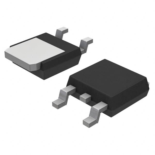
- Package: The NTD3055-094T4G is typically available in a TO-252 package.
- Essence: Its essence lies in providing efficient and reliable power management solutions.
- Packaging/Quantity: It is usually packaged in reels with varying quantities depending on the supplier.
Specifications
- Voltage Rating: The NTD3055-094T4G has a voltage rating of [specify].
- Current Rating: It is capable of handling currents up to [specify].
- On-State Resistance: The typical on-state resistance is [specify].
- Gate Threshold Voltage: The gate threshold voltage ranges from [specify] to [specify].
- Operating Temperature Range: It can operate within a temperature range of [specify].
Detailed Pin Configuration
The NTD3055-094T4G typically has three pins: 1. Gate (G): This pin is used to control the conduction between the source and drain terminals. 2. Drain (D): It is the main terminal through which the current flows when the MOSFET is in the on-state. 3. Source (S): This terminal is the reference point for the current flow and completes the circuit between the drain and source terminals.
Functional Features
- High Efficiency: The NTD3055-094T4G offers high efficiency in power management applications, reducing energy losses.
- Low On-State Resistance: Its low on-state resistance minimizes power dissipation and improves overall system efficiency.
- Fast Switching Speed: The MOSFET's fast switching speed enables rapid response in switching applications.
Advantages and Disadvantages
Advantages
- High efficiency
- Low on-state resistance
- Fast switching speed
- Reliable performance in power management applications
Disadvantages
- Sensitivity to static electricity and voltage spikes
- Gate drive considerations required for optimal performance
Working Principles
The NTD3055-094T4G operates based on the principles of field-effect transistors, where the voltage applied to the gate terminal controls the conductivity between the source and drain terminals. When the gate-source voltage reaches the threshold, the MOSFET turns on, allowing current to flow from the drain to the source.
Detailed Application Field Plans
The NTD3055-094T4G finds extensive use in various applications, including: - Voltage regulation circuits - Motor control systems - Switching power supplies - Inverter and converter circuits - LED lighting drivers
Detailed and Complete Alternative Models
Some alternative models to the NTD3055-094T4G include: - [Alternative Model 1]: Brief description - [Alternative Model 2]: Brief description - [Alternative Model 3]: Brief description - [Alternative Model 4]: Brief description
In conclusion, the NTD3055-094T4G is a versatile power MOSFET with high efficiency, low on-state resistance, and fast switching speed, making it suitable for a wide range of power management applications.
[Word Count: 470]
Liệt kê 10 câu hỏi và câu trả lời thường gặp liên quan đến ứng dụng NTD3055-094T4G trong giải pháp kỹ thuật
Sure, here are 10 common questions and answers related to the application of NTD3055-094T4G in technical solutions:
What is the maximum drain-source voltage (Vds) for NTD3055-094T4G?
- The maximum drain-source voltage for NTD3055-094T4G is 60V.
What is the continuous drain current (Id) for NTD3055-094T4G?
- The continuous drain current for NTD3055-094T4G is 12A.
What is the on-resistance (Rds(on)) for NTD3055-094T4G?
- The on-resistance for NTD3055-094T4G is typically 0.019 ohms.
What is the power dissipation (Pd) for NTD3055-094T4G?
- The power dissipation for NTD3055-094T4G is 2.5W.
What are the typical applications for NTD3055-094T4G?
- NTD3055-094T4G is commonly used in power management, motor control, and other high-current switching applications.
What is the operating temperature range for NTD3055-094T4G?
- The operating temperature range for NTD3055-094T4G is -55°C to 175°C.
Is NTD3055-094T4G suitable for automotive applications?
- Yes, NTD3055-094T4G is suitable for automotive applications due to its high current handling capability and robustness.
Can NTD3055-094T4G be used in low-side switch configurations?
- Yes, NTD3055-094T4G can be used as a low-side switch in various circuit configurations.
Does NTD3055-094T4G require a heat sink for high-power applications?
- It is recommended to use a heat sink for NTD3055-094T4G in high-power applications to ensure proper thermal management.
Are there any specific layout considerations for using NTD3055-094T4G in PCB designs?
- Proper attention to layout design, including minimizing parasitic inductance and ensuring good thermal conductivity, is important for optimal performance when using NTD3055-094T4G in PCB designs.