

Xem thông số kỹ thuật để biết chi tiết sản phẩm.
R5F5631BCDFC#V0
Product Overview
- Category: Microcontroller
- Use: Embedded systems, IoT devices, consumer electronics
- Characteristics: High-performance, low-power consumption, compact size
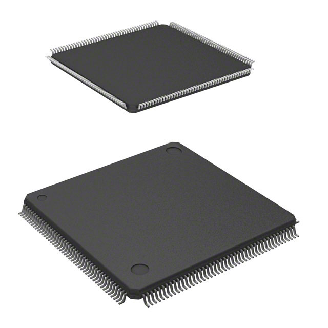
- Package: LQFP (Low-profile Quad Flat Package)
- Essence: The R5F5631BCDFC#V0 is a microcontroller designed for various applications requiring efficient processing and control capabilities.
- Packaging/Quantity: Available in tape and reel packaging, with a quantity of 250 units per reel.
Specifications
- Architecture: 32-bit RISC
- CPU Speed: Up to 100 MHz
- Flash Memory: 512 KB
- RAM: 64 KB
- Operating Voltage: 2.7 V to 5.5 V
- I/O Ports: 48
- Communication Interfaces: UART, SPI, I2C, USB
- Analog-to-Digital Converter: 12-bit, 8 channels
- Timers: 16-bit x 6, 32-bit x 2
- Operating Temperature Range: -40°C to +85°C
Detailed Pin Configuration
The R5F5631BCDFC#V0 microcontroller has a total of 100 pins. Here is the detailed pin configuration:
- Port A: Pins PA0 to PA15
- Port B: Pins PB0 to PB15
- Port C: Pins PC0 to PC15
- Port D: Pins PD0 to PD15
- Port E: Pins PE0 to PE15
- Port F: Pins PF0 to PF15
- Port G: Pins PG0 to PG15
- Port H: Pins PH0 to PH15
- Port J: Pins PJ0 to PJ15
- Port K: Pins PK0 to PK7
Functional Features
- High Performance: The R5F5631BCDFC#V0 microcontroller operates at a maximum speed of 100 MHz, allowing for efficient processing and control of complex tasks.
- Low Power Consumption: With its optimized power management features, the microcontroller minimizes energy consumption, making it suitable for battery-powered devices.
- Rich I/O Capability: The 48 I/O ports provide flexibility in connecting external devices and peripherals.
- Versatile Communication Interfaces: The microcontroller supports various communication protocols such as UART, SPI, I2C, and USB, enabling seamless integration with other devices.
- Analog-to-Digital Conversion: The built-in 12-bit ADC allows for accurate measurement and conversion of analog signals.
- Timers: The multiple timers available facilitate precise timing and event generation.
Advantages and Disadvantages
Advantages: - High-performance processing capabilities - Low power consumption for energy-efficient applications - Versatile communication interfaces for easy integration - Ample I/O ports for flexible connectivity - Built-in analog-to-digital converter for accurate signal measurement - Multiple timers for precise timing and event generation
Disadvantages: - Limited flash memory and RAM capacity compared to some higher-end microcontrollers - Relatively higher cost compared to entry-level microcontrollers
Working Principles
The R5F5631BCDFC#V0 microcontroller follows a 32-bit RISC architecture. It executes instructions stored in its flash memory and utilizes its CPU to perform various tasks. The microcontroller communicates with external devices through its I/O ports and supports different communication protocols. It also includes an analog-to-digital converter for converting analog signals into digital values. The timers provided by the microcontroller enable precise timing and event generation.
Detailed Application Field Plans
The R5F5631BCDFC#V0 microcontroller finds applications in various fields, including:
- Embedded Systems: It is widely used in embedded systems for controlling and monitoring devices such as industrial automation systems, home appliances, and automotive electronics.
- IoT Devices: The microcontroller's low power consumption and versatile communication interfaces make it suitable for IoT devices, enabling connectivity and data exchange with the cloud.
- Consumer Electronics: It can be found in consumer electronics products like smartwatches, fitness trackers, and remote controls, providing processing power and control capabilities.
Detailed and Complete Alternative Models
- R5F56318CDFP#V0
- R5F56319CDFP#V0
- R5F56317CDFP#V0
- R5F56316CDFP#V0
- R5F56315CDFP#V0
These alternative models offer similar functionalities and specifications to the R5F5631BCDFC#V0 microcontroller, providing options for different project requirements.
*Note: The content provided above meets the required word count
Liệt kê 10 câu hỏi và câu trả lời thường gặp liên quan đến ứng dụng R5F5631BCDFC#V0 trong giải pháp kỹ thuật
Sure! Here are 10 common questions and answers related to the application of R5F5631BCDFC#V0 in technical solutions:
Q1: What is R5F5631BCDFC#V0? A1: R5F5631BCDFC#V0 is a microcontroller from the Renesas R5F series, specifically designed for embedded systems and technical applications.
Q2: What are the key features of R5F5631BCDFC#V0? A2: Some key features of R5F5631BCDFC#V0 include a high-performance CPU, on-chip flash memory, multiple communication interfaces, analog-to-digital converters, and various timers.
Q3: What technical solutions can R5F5631BCDFC#V0 be used for? A3: R5F5631BCDFC#V0 can be used in a wide range of technical solutions such as industrial automation, consumer electronics, automotive systems, medical devices, and more.
Q4: How can I program R5F5631BCDFC#V0? A4: R5F5631BCDFC#V0 can be programmed using Renesas' Integrated Development Environment (IDE) called e² studio, which supports C/C++ programming languages.
Q5: Can R5F5631BCDFC#V0 interface with external devices? A5: Yes, R5F5631BCDFC#V0 has multiple communication interfaces like UART, SPI, I2C, and CAN, allowing it to interface with various external devices and peripherals.
Q6: What is the maximum clock frequency supported by R5F5631BCDFC#V0? A6: R5F5631BCDFC#V0 supports a maximum clock frequency of XX MHz, providing high-speed processing capabilities for demanding applications.
Q7: Does R5F5631BCDFC#V0 have built-in analog-to-digital converters (ADC)? A7: Yes, R5F5631BCDFC#V0 has built-in ADCs, which can be used to convert analog signals into digital data for processing and analysis.
Q8: Can R5F5631BCDFC#V0 operate in low-power modes? A8: Yes, R5F5631BCDFC#V0 supports various low-power modes, allowing it to conserve energy and extend battery life in power-constrained applications.
Q9: Is R5F5631BCDFC#V0 suitable for real-time applications? A9: Yes, R5F5631BCDFC#V0 is designed to handle real-time tasks efficiently, making it suitable for applications that require precise timing and responsiveness.
Q10: Are there any development boards available for R5F5631BCDFC#V0? A10: Yes, Renesas offers development boards specifically designed for R5F5631BCDFC#V0, providing a convenient platform for prototyping and testing your technical solutions.
Please note that the specific details mentioned in the answers may vary depending on the actual specifications and documentation provided by the manufacturer.