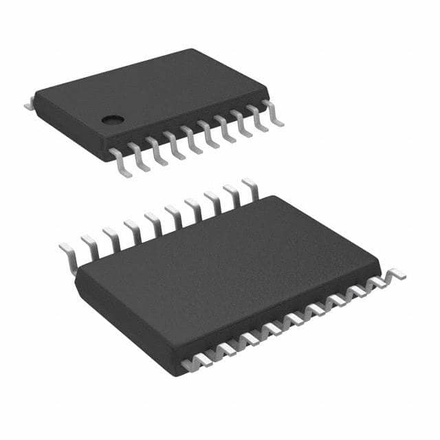
Xem thông số kỹ thuật để biết chi tiết sản phẩm.

Encyclopedia Entry: 74LVC244ATTR
Product Overview
- Category: Integrated Circuit (IC)
- Use: Signal Buffer/Driver
- Characteristics: Low Voltage CMOS Octal Buffer/Line Driver with 3-State Outputs
- Package: TSSOP (Thin Shrink Small Outline Package)
- Essence: The 74LVC244ATTR is a high-performance buffer/driver IC designed for low voltage applications.
- Packaging/Quantity: Available in reels, typically containing 2500 units.
Specifications
- Supply Voltage Range: 1.65V to 5.5V
- High-Speed Operation: 20 ns maximum propagation delay
- Output Drive Capability: ±24 mA
- Input Voltage Levels: Compatible with TTL and CMOS logic levels
- Operating Temperature Range: -40°C to +85°C
Detailed Pin Configuration
The 74LVC244ATTR has a total of 20 pins, which are arranged as follows:
+--\/--+
   A1 --|1    20|-- VCC
   B1 --|2    19|-- B2
   A2 --|3    18|-- A3
   B3 --|4    17|-- B4
   A4 --|5    16|-- A5
   B5 --|6    15|-- B6
   A6 --|7    14|-- A7
   B7 --|8    13|-- B8
  GND --|9    12|-- OE#
  DIR --|10   11|-- GND
        +------+
Functional Features
- Octal Buffer/Line Driver: Provides eight independent buffers with 3-state outputs.
- 3-State Outputs: Allows multiple devices to share a common bus without interference.
- Low Voltage Operation: Suitable for battery-powered devices and low voltage systems.
- High-Speed Operation: Enables efficient data transfer in time-critical applications.
- TTL/CMOS Compatible: Can interface with both TTL and CMOS logic levels.
Advantages and Disadvantages
Advantages: - Low voltage operation extends battery life in portable devices. - High-speed operation enables fast data transmission. - 3-state outputs facilitate bus sharing among multiple devices.
Disadvantages: - Limited output drive capability compared to some other buffer/driver ICs. - May not be suitable for high-power applications due to its low voltage design.
Working Principles
The 74LVC244ATTR operates by receiving input signals on the A1-A7 pins and driving corresponding output signals on the B1-B8 pins. The DIR pin controls the direction of data flow, while the OE# pin enables or disables the outputs. When the OE# pin is active (low), the outputs are enabled, allowing the data to pass through. Conversely, when the OE# pin is inactive (high), the outputs are disabled, entering a high-impedance state.
Detailed Application Field Plans
The 74LVC244ATTR is commonly used in various applications, including but not limited to: - Microcontroller interfacing - Data communication systems - Memory address decoding - Bus drivers for computer systems - Industrial automation
Detailed and Complete Alternative Models
Some alternative models that can be considered as alternatives to the 74LVC244ATTR include: - 74HC244: Similar octal buffer/driver IC with TTL-compatible inputs. - SN74LV244A: Low voltage octal buffer/driver IC with 3-state outputs. - CD74HCT244: High-speed CMOS octal buffer/driver IC with TTL-compatible inputs.
In conclusion, the 74LVC244ATTR is a versatile buffer/driver IC designed for low voltage applications. Its high-speed operation, 3-state outputs, and compatibility with TTL and CMOS logic levels make it suitable for various electronic systems. However, its limited output drive capability and low voltage design may restrict its use in certain high-power applications.
Liệt kê 10 câu hỏi và câu trả lời thường gặp liên quan đến ứng dụng 74LVC244ATTR trong giải pháp kỹ thuật
Sure! Here are 10 common questions and answers related to the application of 74LVC244ATTR in technical solutions:
Q: What is the purpose of the 74LVC244ATTR? A: The 74LVC244ATTR is a buffer/line driver IC used to amplify and control digital signals.
Q: What voltage levels does the 74LVC244ATTR support? A: The 74LVC244ATTR supports voltage levels from 1.65V to 5.5V.
Q: Can the 74LVC244ATTR be used for bidirectional communication? A: No, the 74LVC244ATTR is unidirectional and can only be used for one-way signal transmission.
Q: How many channels does the 74LVC244ATTR have? A: The 74LVC244ATTR has 8 channels, allowing it to handle 8 separate signals.
Q: What is the maximum output current of the 74LVC244ATTR? A: The 74LVC244ATTR can provide a maximum output current of 24mA per channel.
Q: Can the 74LVC244ATTR be used with both CMOS and TTL logic levels? A: Yes, the 74LVC244ATTR is compatible with both CMOS and TTL logic levels.
Q: Does the 74LVC244ATTR have any built-in protection features? A: Yes, the 74LVC244ATTR has built-in ESD protection to safeguard against electrostatic discharge.
Q: What is the operating temperature range of the 74LVC244ATTR? A: The 74LVC244ATTR can operate within a temperature range of -40°C to +125°C.
Q: Can the 74LVC244ATTR be used in high-speed applications? A: Yes, the 74LVC244ATTR is designed for high-speed operation and can handle frequencies up to several hundred megahertz.
Q: What is the power supply voltage range for the 74LVC244ATTR? A: The 74LVC244ATTR requires a power supply voltage between 1.65V and 5.5V.
Please note that these answers are general and may vary depending on the specific datasheet and manufacturer's specifications of the 74LVC244ATTR.

