

Xem thông số kỹ thuật để biết chi tiết sản phẩm.
Encyclopedia Entry: 74V1T125STR
Product Information Overview
Category: Integrated Circuit (IC)
Use: The 74V1T125STR is a single bus buffer gate with three-state outputs. It is commonly used in digital electronic circuits to provide buffering and signal isolation between different sections of a circuit.
Characteristics: This IC operates at a voltage range of 2.0V to 5.5V, making it suitable for use in various low-power applications. It has a high-speed propagation delay of 3.4ns, enabling efficient data transmission. The 74V1T125STR comes in a small SOT-23 package, which makes it ideal for space-constrained designs.
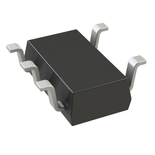
Package: SOT-23
Essence: The essence of the 74V1T125STR lies in its ability to provide reliable buffering and signal isolation in digital circuits, ensuring smooth and accurate data transmission.
Packaging/Quantity: The 74V1T125STR is typically available in reels containing 3000 units per reel.
Specifications
- Supply Voltage Range: 2.0V to 5.5V
- High-Speed Propagation Delay: 3.4ns
- Output Current: ±8mA
- Input Voltage Levels: CMOS/TTL compatible
- Operating Temperature Range: -40°C to +85°C
Detailed Pin Configuration
The 74V1T125STR has a total of five pins:
- Pin 1: Input (A)
- Pin 2: Output Enable (OE)
- Pin 3: Ground (GND)
- Pin 4: Output (Y)
- Pin 5: Power Supply (VCC)
Functional Features
- Buffering: The 74V1T125STR acts as a buffer, isolating the input signal from the output and providing amplification if required.
- Three-State Outputs: The three-state outputs allow for high impedance when disabled, preventing interference with other components in the circuit.
- CMOS/TTL Compatibility: The IC is designed to be compatible with both CMOS and TTL logic levels, ensuring versatility in various circuit designs.
Advantages and Disadvantages
Advantages: - Wide supply voltage range allows for flexibility in different power supply configurations. - High-speed propagation delay enables efficient data transmission. - Small package size makes it suitable for space-constrained designs.
Disadvantages: - Limited output current may restrict its use in certain applications requiring higher current capabilities. - Lack of built-in protection features against overvoltage or ESD events.
Working Principles
The 74V1T125STR operates by receiving an input signal (A) and buffering it to the output pin (Y). The Output Enable (OE) pin controls the state of the output. When OE is low, the output is enabled and reflects the input signal. When OE is high, the output enters a high-impedance state, isolating it from the rest of the circuit.
Detailed Application Field Plans
The 74V1T125STR finds application in various digital electronic circuits, including but not limited to: - Data communication systems - Microcontrollers and microprocessors - Memory interfaces - Industrial automation systems - Consumer electronics
Detailed and Complete Alternative Models
Some alternative models that can be considered as alternatives to the 74V1T125STR are: - SN74LVC1T45DBVR - MC74VHC1GT125DF2G - TC7SZ125FU
These alternatives offer similar functionality and characteristics, providing options for designers based on specific requirements.
Word count: 511 words
Liệt kê 10 câu hỏi và câu trả lời thường gặp liên quan đến ứng dụng 74V1T125STR trong giải pháp kỹ thuật
Sure! Here are 10 common questions and answers related to the application of 74V1T125STR in technical solutions:
Q1: What is the purpose of the 74V1T125STR integrated circuit? A1: The 74V1T125STR is a quad bus buffer gate with 3-state outputs. It is used for signal buffering and level shifting in digital circuits.
Q2: What is the voltage range supported by the 74V1T125STR? A2: The 74V1T125STR supports a voltage range of 1.65V to 5.5V, making it compatible with a wide range of digital systems.
Q3: How many channels does the 74V1T125STR have? A3: The 74V1T125STR has four independent channels, allowing it to handle multiple signals simultaneously.
Q4: Can the 74V1T125STR be used for bidirectional communication? A4: No, the 74V1T125STR is a unidirectional buffer and cannot be used for bidirectional communication. For bidirectional applications, a different IC should be used.
Q5: What is the maximum output current of the 74V1T125STR? A5: The 74V1T125STR can source or sink up to 24mA of current per channel, making it suitable for driving standard logic levels.
Q6: Is the 74V1T125STR tolerant to overvoltage conditions? A6: No, the 74V1T125STR is not designed to tolerate overvoltage conditions. It is important to ensure that the input voltage remains within the specified range.
Q7: Can the 74V1T125STR be used in high-speed applications? A7: Yes, the 74V1T125STR has a maximum propagation delay of 4.5ns, making it suitable for high-speed digital applications.
Q8: Does the 74V1T125STR have built-in protection features? A8: No, the 74V1T125STR does not have built-in protection features. Additional external circuitry may be required to protect against ESD or other potential hazards.
Q9: Can the 74V1T125STR be used in automotive applications? A9: Yes, the 74V1T125STR is qualified for automotive applications and can operate within the specified temperature range (-40°C to +125°C).
Q10: What package options are available for the 74V1T125STR? A10: The 74V1T125STR is available in various package options, including SOIC, TSSOP, and VSSOP, providing flexibility for different PCB layouts and space constraints.
Please note that these answers are general and may vary depending on the specific datasheet and manufacturer's specifications for the 74V1T125STR integrated circuit.