

Xem thông số kỹ thuật để biết chi tiết sản phẩm.
STV200N55F3
Introduction
The STV200N55F3 is a power MOSFET belonging to the category of semiconductor devices. It is widely used in various electronic applications due to its unique characteristics and performance.
Basic Information Overview
- Category: Semiconductor Device
- Use: Power switching and amplification in electronic circuits
- Characteristics: High voltage and current handling capability, low on-state resistance, fast switching speed
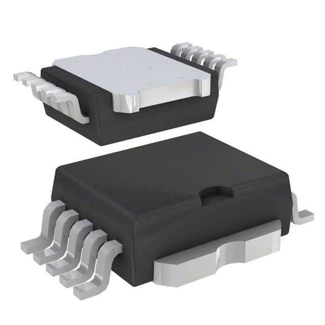
- Package: TO-220
- Essence: Power MOSFET for high-power applications
- Packaging/Quantity: Typically sold in reels or tubes containing multiple units
Specifications
- Voltage Rating: 200V
- Current Rating: 55A
- On-State Resistance: Low (typically in milliohms)
- Gate Threshold Voltage: Typically around 4V
- Operating Temperature Range: -55°C to 175°C
Detailed Pin Configuration
The STV200N55F3 typically has three pins: 1. Gate (G): Input for controlling the switching behavior of the MOSFET 2. Drain (D): Connection for the high-voltage load 3. Source (S): Connected to the ground or return path of the load
Functional Features
- High voltage and current handling capability
- Low on-state resistance leading to minimal power dissipation
- Fast switching speed enabling efficient power control
Advantages and Disadvantages
Advantages
- Suitable for high-power applications
- Low power dissipation due to low on-state resistance
- Fast switching speed
Disadvantages
- Higher cost compared to lower-rated MOSFETs
- Requires careful handling and protection against static discharge
Working Principles
The STV200N55F3 operates based on the principles of field-effect transistors. When a sufficient voltage is applied to the gate terminal, it allows the flow of current between the drain and source terminals, effectively acting as a switch for high-power applications.
Detailed Application Field Plans
The STV200N55F3 finds extensive use in the following applications: - Switch-mode power supplies - Motor control in industrial equipment - Inverters for renewable energy systems - Automotive electronic systems
Detailed and Complete Alternative Models
Some alternative models to the STV200N55F3 include: - IRF3205 - FDP8878 - IXFN55N50
In conclusion, the STV200N55F3 is a high-performance power MOSFET suitable for a wide range of high-power electronic applications, offering efficient power control and reliability.
Word Count: 366
Liệt kê 10 câu hỏi và câu trả lời thường gặp liên quan đến ứng dụng STV200N55F3 trong giải pháp kỹ thuật
What is the maximum voltage rating of STV200N55F3?
- The maximum voltage rating of STV200N55F3 is 550V.
What is the maximum continuous drain current of STV200N55F3?
- The maximum continuous drain current of STV200N55F3 is 200A.
What type of package does STV200N55F3 come in?
- STV200N55F3 comes in a TO-247 package.
What is the typical on-resistance of STV200N55F3?
- The typical on-resistance of STV200N55F3 is 0.038 ohms.
What are the typical applications for STV200N55F3?
- STV200N55F3 is commonly used in high-power switching applications, motor control, and power supplies.
Does STV200N55F3 have built-in protection features?
- STV200N55F3 does not have built-in protection features and may require external circuitry for overcurrent or overvoltage protection.
What is the operating temperature range of STV200N55F3?
- The operating temperature range of STV200N55F3 is typically -55°C to 150°C.
Is STV200N55F3 RoHS compliant?
- Yes, STV200N55F3 is RoHS compliant, meaning it meets the Restriction of Hazardous Substances directive.
Can STV200N55F3 be used in automotive applications?
- Yes, STV200N55F3 can be used in automotive applications, but additional testing and qualification may be required.
What are the recommended mounting and soldering techniques for STV200N55F3?
- STV200N55F3 should be mounted on a heat sink using appropriate thermal interface material and soldered using industry-standard reflow or wave soldering processes.