

Xem thông số kỹ thuật để biết chi tiết sản phẩm.
ADS42LB69IRGCT
Product Overview
Category: Integrated Circuit (IC)
Use: The ADS42LB69IRGCT is a high-speed analog-to-digital converter (ADC) designed for use in various applications that require precise and fast conversion of analog signals into digital data. It is commonly used in communication systems, medical imaging devices, radar systems, and other high-performance electronic equipment.
Characteristics: - High-speed conversion: The ADS42LB69IRGCT can convert analog signals into digital data at a very high speed, making it suitable for applications that require real-time processing. - High resolution: It offers a high resolution of up to 16 bits, ensuring accurate representation of the analog input signal. - Low power consumption: Despite its high performance, the ADC consumes relatively low power, making it energy-efficient. - Wide input voltage range: It supports a wide input voltage range, allowing it to handle various signal levels. - Low noise and distortion: The ADC provides excellent signal-to-noise ratio and low distortion, ensuring high-quality conversion.
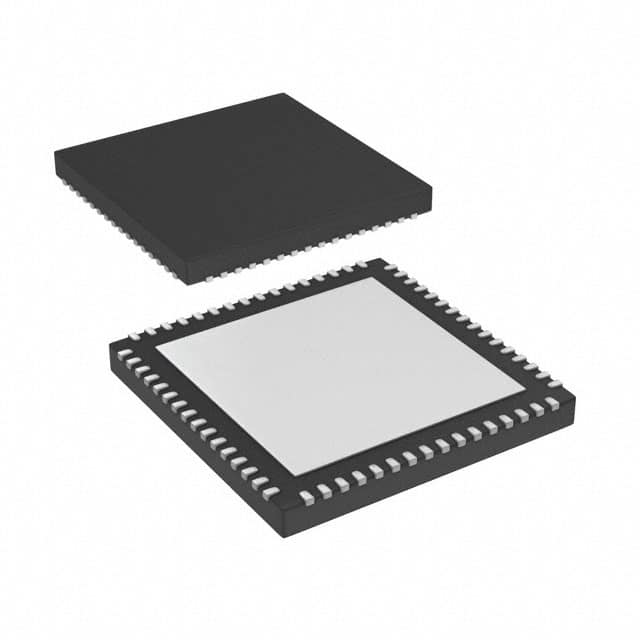
Package: The ADS42LB69IRGCT is available in a small form factor package, which facilitates easy integration into electronic systems. The package type is RGCT.
Essence: The essence of the ADS42LB69IRGCT lies in its ability to accurately and quickly convert analog signals into digital data, enabling efficient processing and analysis of the acquired information.
Packaging/Quantity: The ADC is typically sold in reels or trays, with a quantity of 250 units per reel/tray.
Specifications
- Resolution: Up to 16 bits
- Sampling Rate: Up to 500 Mega Samples Per Second (MSPS)
- Input Voltage Range: ±2 V
- Power Supply: 3.3 V
- Operating Temperature Range: -40°C to +85°C
- Package Type: RGCT
Detailed Pin Configuration
The ADS42LB69IRGCT has a total of 64 pins, which are assigned specific functions. The pin configuration is as follows:
(Pin Number - Pin Name - Function) 1. VREFP - Positive Reference Voltage Input 2. VREFN - Negative Reference Voltage Input 3. VINP0A - Analog Input Channel 0A (Positive) 4. VINN0A - Analog Input Channel 0A (Negative) 5. VINP0B - Analog Input Channel 0B (Positive) 6. VINN0B - Analog Input Channel 0B (Negative) 7. VINP1A - Analog Input Channel 1A (Positive) 8. VINN1A - Analog Input Channel 1A (Negative) 9. VINP1B - Analog Input Channel 1B (Positive) 10. VINN1B - Analog Input Channel 1B (Negative) 11. ... ... 64. GND - Ground
Functional Features
- Dual-channel operation: The ADC supports dual-channel operation, allowing simultaneous conversion of two analog input signals.
- Programmable gain amplifier: It includes a programmable gain amplifier that enables amplification of weak input signals to improve the overall signal-to-noise ratio.
- Digital output interface: The ADC provides a digital output interface, typically using a high-speed serial interface such as LVDS or JESD204B, for easy integration with digital processing systems.
- Built-in digital filters: It incorporates digital filters that can be configured to enhance the quality of the converted digital data.
Advantages and Disadvantages
Advantages: - High-speed conversion capability - High resolution for accurate signal representation - Low power consumption - Wide input voltage range - Low noise and distortion
Disadvantages: - Relatively higher cost compared to lower-performance ADCs - Requires careful PCB layout and signal integrity considerations for optimal performance
Working Principles
The ADS42LB69IRGCT utilizes a pipeline architecture for high-speed analog-to-digital conversion. It consists of multiple stages, each performing a partial conversion of the input signal. The converted data from each stage is then combined to produce the final digital output.
The analog input signal is first amplified by the programmable gain amplifier (PGA) to match the desired input range. The amplified signal is then sampled at a high rate using a sample-and-hold circuit. The sampled values are subsequently processed through the pipeline stages, where each stage performs a portion of the conversion process.
In each stage, the analog signal is successively approximated by comparing it with a set of reference voltages. The resulting digital codes from each stage are combined to form the final digital output, which represents an accurate digital representation of the original analog input signal.
Detailed Application Field Plans
The ADS42LB69IRGCT finds applications in various fields that require high-speed and high-resolution analog-to-digital conversion. Some specific application areas include:
1
Liệt kê 10 câu hỏi và câu trả lời thường gặp liên quan đến ứng dụng ADS42LB69IRGCT trong giải pháp kỹ thuật
Sure! Here are 10 common questions and answers related to the application of ADS42LB69IRGCT in technical solutions:
Q: What is the ADS42LB69IRGCT? A: The ADS42LB69IRGCT is a high-performance analog-to-digital converter (ADC) designed for applications that require high-speed data acquisition.
Q: What is the maximum sampling rate of the ADS42LB69IRGCT? A: The ADS42LB69IRGCT can achieve a maximum sampling rate of 250 Mega-samples per second (MSPS).
Q: What is the resolution of the ADC? A: The ADS42LB69IRGCT has a resolution of 16 bits, allowing it to capture fine details in the analog signal.
Q: What is the input voltage range of the ADC? A: The ADS42LB69IRGCT has a differential input voltage range of ±0.5 V, making it suitable for a wide range of input signals.
Q: Can the ADS42LB69IRGCT be used in low-power applications? A: Yes, the ADS42LB69IRGCT features a power-down mode that reduces power consumption when the ADC is not actively converting.
Q: Does the ADC support multiple output interfaces? A: Yes, the ADS42LB69IRGCT supports both parallel and serial LVDS (Low-Voltage Differential Signaling) output interfaces, providing flexibility in system integration.
Q: What is the typical noise performance of the ADC? A: The ADS42LB69IRGCT offers excellent noise performance with a signal-to-noise ratio (SNR) of up to 75 dBFS at a 70 MHz input frequency.
Q: Can the ADC be used in high-frequency applications? A: Yes, the ADS42LB69IRGCT has a wide input bandwidth of up to 500 MHz, making it suitable for high-frequency signal acquisition.
Q: Does the ADC require an external reference voltage? A: Yes, the ADS42LB69IRGCT requires an external reference voltage for accurate conversion. It supports both internal and external reference options.
Q: What are some typical applications of the ADS42LB69IRGCT? A: The ADS42LB69IRGCT is commonly used in applications such as wireless communications, radar systems, medical imaging, and test and measurement equipment.
Please note that these answers are general and may vary depending on specific implementation requirements.